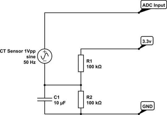
first circuit
The purpose of the first one is to build a stable virtual ground at 3.3 V / 2, which you use as reference potential for your sensor.
Your ADC senses the voltage over the sensor. It's important that the ADC has a high input impedance (>> 100 kΩ, which is relatively much for low-noise ADCs), otherwise it doesn't work, because the sensor then starts to shift the virtual ground instead of the ADC input.
second circuit
Opamp is in a negative feedback configuration, so that the voltage difference at the inputs becomes 0 V. Since no current can flow into an Opamp input, that means that the inverting input is pulled to 3.3 V / 2.
From that directly follows that on the left hand side of R4, there's V_sensor, on the right hand side always 3.3 V / 2.
Therefore, R4 conducts a current of
$$I_4=\frac{V_\text{sensor}-3.3\,\text{V}/2}{R_4}$$
Since that current can't go anywhere, the current through R3 is \$I_3=I_4\$ and hence the voltage at the right hand side of R3 is the 3.3 V / 2 on its left end, plus the voltage across R3, so
\begin{align}
V_\text{ADC} &= 3.3 \,\text{V} + I_3 \cdot R_3 \\
&\overset{I_3=I_4}= 3.3 \,\text{V} + I_4 \cdot R_3 \\
&= 3.3 \,\text{V} + \frac{V_\text{sensor}-3.3\,\text{V}/2}{R_4}R_3\\
&\overset{R_3=R_4}=3.3 \,\text{V} + V_\text{sensor}-3.3\,\text{V}/2\\
&=3.3 V /2 + V_\text{sensor}
\end{align}
which is the same as for the first circuit, but with an important difference:
The internal source impedance of that \$V_\text{ADC}\$ voltage source is no longer defined by the virtual ground and the current sensor, but by the output impedance of the opamp!
Hence, you can use opamps with much lower input impedances; in fact, what you often do is even have a termination resistor really close to the ADC input, and use the ADC to measure the voltage across that, instead of terminating the line into the ADC itself.
That has the effect that noise voltage (whose sources we typically model as high-internal impedance voltage sources) "breaks down" over the strong termination resistor, whereas your signal of interest is "strong enough" and can be, without degradation, be measured.
Also the phase of the signal is inverted which I think it doesn't bother much.
Not quite sure what you want to measure, but it would bother me very much if my signal's phase was changed. You need to account for anything like that!