After looking into this a bit more, I think I have a better answer than my comment above.
Since the LM148 is (as the datasheet says) "a true quad 741", I had a look at the actual schematic of the famous 741 opamp. Which you shouldn't be using, read here why. Of course for educational purposes, studying the 741 (or LM148) is fine.
This site has an excellent and detailed analysis of the 741. Here's the internal schematic:
Now we can see that the PNP-diode on top of the NPN input pair is actually part of a current mirror.
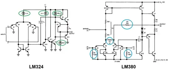
So the schematic of the LM148 from your question appears to be a simplification of the real schematic.
That PNP-diode copies the (DC) current flowing in the input stage, the copied current comes out of Q9. PNP Q12, the 39 k resistor and NPN Q11 form a crude DC biasing reference. NPNs Q10 and Q11 form another mirror which copies this bias current, then at the collectors of Q9 and Q10 this DC biasing current is compared against the biasing current of the input stage. That makes the voltage at the Bases of Q3 and Q4 go up/down and that then regulates the DC biasing current of the input stage.
So that Q8, that PNP diode, is part of the circuit that sets the DC biasing current of the input stage.
From its schematic, the LM148 does appear to use a somewhat different biasing scheme for its input stage. Often, details are left out in these "internal circuits" on datasheets so we cannot be sure what exactly goes on in the LM148. It might be that they kept PNP Q8 in place to not change the behavior of the input stage compared to the 741.

