8

I've been trying to get the SPI1 on the STM32F103C8 (Blue Pill board) working correctly for some time now. As I'm just starting to learn ARM, I am simply trying to shift data to a 74HC595 shift register and latch it to light up a byte of LEDs. I am not reading back any data, so I only have MOSI, SCK and SS lines.

At first I wasn't getting anything out, but reading some online examples I could fix these first problems to get the communication going (I needed to correctly set GPIOA pins and set software SS).

The main problem right now is that if I don't include pull-up resistors on all lines (MOSI, SCK, and SS) the microcontroller doesn't output anything on any line (checked with a scope). On top of this, after adding pull-up resistors the rise time on the pulses is very slow so I can't use too high a frequency (with 10 kΩ pull-up resistors I'm limited to about 250 kHz SCK, and switching to 330 Ω about 4 MHz). I am working on a breadboard, but even then with AVR and messier wiring I could get a 4 MHz SPI working no problem without any added resistors and the waveforms were cleaner.

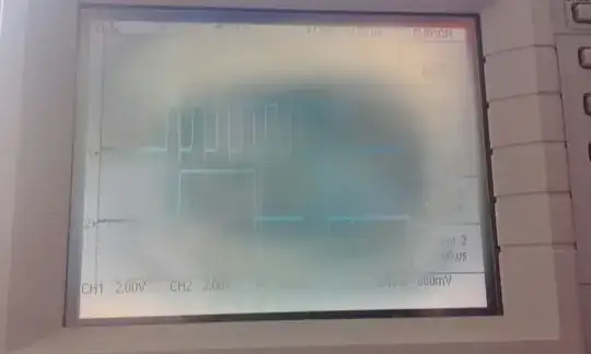
Here are two pictures (sorry for the abysmal state of my scope screen) transmitting the byte 0b01110010 at a 250 kHz clock. The top trace is SCK and the bottom is MOSI. The first picture is with 10 kΩ pull-up resistors and the second with 330 Ω pull-up resistors that make the waveforms much nicer (but they shouldn't be needed).

I'd appreciate some help to figure out what's going on.

10 kΩ pull-up resistors and 250 kHz clock

330 Ω pull-up resistors and 250 kHz make waveform a lot nicer

The relevant parts of my code are:

#define SS_LOW        GPIOA->BSRR |= 1 << 4 + 16;
#define SS_HIGH        GPIOA->BSRR |= 1 << 4;

// SPI GPIO configuration
RCC->APB2ENR |= RCC_APB2ENR_IOPAEN;
GPIOA->CRL |= 0b0011 << 4 * 4;    // Set pin A4 as PP out 50mHz for SS
GPIOA->CRL |= 0b1011 << 5 * 4;    // Set pin A5 AltFunc PP out 50mHz for SCK
GPIOA->CRL |= 0b1011 << 7 * 4;    // Set pin A7 AltFunc PP out 50mHz for MOSI
SS_HIGH;

// SPI1 configuration
RCC->APB2ENR |= RCC_APB2ENR_SPI1EN;        // Enable SPI1 clock
SPI1->CR1 |= SPI_CR1_SSM;        // Software SS
SPI1->CR1 |= SPI_CR1_SSI;
SPI1->CR1 |= SPI_CR1_BR_0;        // Set prescaler
SPI1->CR1 |= SPI_CR1_BR_1;
SPI1->CR1 |= SPI_CR1_BR_2;
SPI1->CR1 |= SPI_CR1_MSTR;        // Master mode
SPI1->CR1 |= SPI_CR1_SPE;        // Enable SPI

// Transmit byte
SS_LOW;
SPI1->DR = 0b01110010;
while(!(SPI1->SR & SPI_SR_TXE));
while(SPI1->SR & SPI_SR_BSY);
SS_HIGH;
Peter Mortensen
  • 1,676
  • 3
  • 17
  • 23
jjpprr
  • 163
  • 1
  • 6
  • What is your setup? How are your wires connected? Are you using a custom board or a breadboard? – Tarick Welling May 28 '19 at 14:32
  • I'm using a breadboard. The 74hc595 is powered from the 3.3V of the blue pill board (this one to be precise: https://revspace.nl/File:Bluepill.jpg). The only wires going from and to the shift register are MOSI, SCK and SS. I'm positive the wiring is correct, I checked it numerous times (and once again before answering you). – jjpprr May 28 '19 at 14:44

1 Answers1

12

You should reset the value of the pins you are changing before setting the bits.

The reset value of GPIOA_CRL is 0x4444 4444. So each pin is initialized with 0b0100, if you do a |= 0b0011 you end up with 0b0111 which is an open drain output. Same with 0b1011 becomes 0b1111 and that is an alternate function open drain.

So you need to do something like this:

// Reset pin configuration
GPIOA->CRL &= ~(0b1111 << 4 * 4);  // Reset Pin A4
GPIOA->CRL &= ~(0b1111 << 5 * 4);  // Reset Pin A5
GPIOA->CRL &= ~(0b1111 << 7 * 4);  // Reset Pin A7
GPIOA->CRL |= 0b0011 << 4 * 4;  // Set pin A4 as PP out 50mHz for SS
GPIOA->CRL |= 0b1011 << 5 * 4;  // Set pin A5 AltFunc PP out 50mHz for SCK
GPIOA->CRL |= 0b1011 << 7 * 4;  // Set pin A7 AltFunc PP out 50mHz for MOSI
Arsenal
  • 17,464
  • 1
  • 32
  • 59
  • This was it!! Thank you so much, I knew it was going to be something so simple. Should have read the first line on GPIOA_CRL of the datasheet, I just assumed reset value was all zeros. It now works a charm. – jjpprr May 28 '19 at 14:48
  • @jjpprr well it took me a while to realize as well :-) Glad I could help. If you are going to use I²C on the F103, be ready for a rough ride, I remember it being horrible. – Arsenal May 28 '19 at 14:56
  • :O will take that into account, after getting USART up and running it will be I2Cs turn. Thanks for the heads up. – jjpprr May 28 '19 at 14:58
  • The thing which stands out most profoundly where the interrupts I was getting without any interrupt source which messed up my state machine. In the end I went for an approach which doesn't use I²C interrupts at all (but the DMA interrupt for the end of transmission) and just polls the I²C bits for start and stuff, but my application had to wait for I²C to finish anyway, so I wasn't gaining time with interrupts anyway. – Arsenal May 28 '19 at 15:06
  • Was this only with the F103 or also other stm32 chips? Because my plan was to use it just to get the hang of stm32 ICs but then move on to the F091 for small projects and F446 for more demanding stuff. – jjpprr May 28 '19 at 15:10
  • @jjpprr I have encountered two completely different I²C implementations in the STM32 so far. One of the F103 which I also had in the F401 (I think) and one in the F051 which I encountered in the L476 and L451 (I think). So there are different peripherals around. And there are slight alterations between chips. I guess if you aren't required to write your own drivers, using the Cube HAL or Cube LL might be a faster approach. But if you like the challenge of implementing it yourself be sure to read the manual closely and if you transfer something check the register map if it is the same (my way). – Arsenal May 28 '19 at 15:14