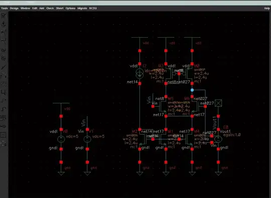
I am currently trying to reduce the offset voltage of the circuit attached below to less than +/- 2mV over a 1V to 4V input range.
I have a few constraints for this task:
I can use
nmos,pmosandpmos4but can't usenmos4as the fabrication process does not support separate bulks for NMOS transistors.I cannot use controlled sources e.g (
vcvs,vccs,ccvs,cccs) except when calculating VoffsetI can only use one
VdcforVddand oneVdcforVinand use onlyidcfor biasingUse at least 100nA bias current in all transistors
So far I have tried adding cascodes to the circuit to reduce this offset voltage but no luck. I would really appreciate it if someone could point me in the right direction regarding this task. Thank you.
Voltage Follower Circuit:
