7

enter image description here

Hi does anybody know what's the purpose of the Q1 and Q2 transistors, sounds to me like they are constant current sources. Am I wrong?

Could somebody explain me the purpose of those Q1 and Q2 transistor configuration there?

Note, This is a simple preamp circuit.

Standard Sandun
  • 1,695
  • 2
  • 23
  • 38
  • 4
    No, they are constant voltage sources to first approximation, not constant current. They are basically used as diodes, but for the voltage drop, not the rectifying property. – Olin Lathrop Oct 06 '12 at 23:05
  • 1
    Holy C**p! This question (and the answers) exactly solved a problem that I m dealing with right now. Awesome! –  Oct 10 '12 at 19:46
  • Good to hear that David Kessner – Standard Sandun Oct 12 '12 at 07:02

3 Answers3

7

They act like a diode to bias the output transistor bases. They are like a Vbe multiplier (also known as a rubber diode - see here) without the multiplication (i.e R1 0Ω, R2 infinite in the diagram below), so the drop is ~0.6V.
In a class AB or class B amp they are often used to provide a trimmable ~2*Vbe drop to bias the output transistors:

enter image description here

Note the input is at the upper side, so one ~2*Vbe multiplier (~1.4V, depending on desired bias)) can be used. In your circuit it's in the middle, so you need 2 drops each of around 0.6V.

Oli Glaser
  • 54,990
  • 3
  • 76
  • 147
  • 1
    I don't think the arrangement has anything to do with the rubber diode. The transistors are literally used as passive diodes; they are not an active circuit that can be adjusted to an arbitrary voltage drop. – Kaz Oct 10 '12 at 18:23
  • @Kaz - you're right they just provide a diode drop, probably to compensate thermally as Richman mentions. I probably focused unnecessarily on the Vbe multiplier ("Rubber diode") aspect, I just wanted to point out how it works (i.e. why the transistor doesn't go into saturation and stays at 0.6V drop, which is the same as a Vbe multiplier without the base emitter resistor so there is no multiplication) – Oli Glaser Oct 10 '12 at 19:27
  • In the diode-connected BJT, the VCE stays at around 0.6V because CE is connected in parallel to BE forcing VCE to be equal to VBE. Saturation is avoided because VCB is zero (since B and C are connected), and so the CB junction cannot be forward biased. Also VCE is held at VBE, which is above what the saturation VCE would be. I see how this can be regarded as a special case of the rubber diode, where R1 = 0 and R2 = infinite. But that alone doesn't explain the lack of saturation. Saturation would simply need some (impossible) multiplier of < 1 since saturation doesn't occur at VCE = VBE. – Kaz Oct 10 '12 at 23:55
  • @Kaz, yes that's my basic point (pretty badly put it appears - I'm beginning to wish I'd never mentioned the rubber diode now :-) ), that saturation cannot occur because the collector is tied to base. I was trying to highlight what happens if you connect the collector to the base. – Oli Glaser Oct 11 '12 at 14:40
3

Q1/Q2 are transistors configured as diodes. Which drive the bases of Q3/Q4 (respectively) with a Vf offset that is +Vf/-Vf from pin 1 of IC1. This would be an class AB amplifier and the offset bias provided by Q1/Q2 reduces the shoot through current and isolates Q3/ base from q4 base. THe feedback for the amplifier is after the amplification provided by Q3/Q4 which will correct for the overlap distortion. the output will swing to within a Vce of each rail.

placeholder
  • 29,982
  • 10
  • 63
  • 110
3

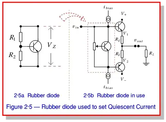
Q1/Q2 's main purpose is temperature compensation of Vbe of the output drivers. In order for this to work effectively, they must be connected to a common heatsink. so the diode drops cancel out within 1% and prevent thermal runaway. The other answers are also correct but the main purpose is to prevent thermal runaway with compensation.

= added = To prevent thermal runaway with the Q3 & Q4 becoming biased at the same time, you want the DC base current constant over temperature and supply variations. We know Vbe has a NTC or negative temperature coefficient, so Vbe drops with rising T so a fixed voltage bias would result more DC emitter current which may increase T and thus a positive feedback thermal loop called runaway. Hence the diodes Q1/Q2 will produce a similar voltage to Q3/Q4 as a function of temperature. The differences include the ESR of Vbe and the junction temperatures. ( Q1 vs Q3 & Q2 vs Q4 ) Ideal circuit design will minimize these differences. The self-destructive runaway can get triggered by low headphone resistance at high volume levels causing thermal rise but be ok otherwise. The output current limiting resistor is designed to reduce that risk.

Given that the Q3/Q4 also has an emitter resistor, the risk for thermal runaway is also lowered but the amount of crossover distortion is increased with frequency due to reduction in loop gain.

Tony Stewart EE75
  • 1
  • 3
  • 54
  • 182