10

Can/Are processors be designed using different technologies ? What I mean here is: in, for example, Intel's 28nm processors, are all the gates in that processor built in 28nm technology or are only the most critical parts of that processor built in 28nm, the other, much much less critical parts being designed in other much less expensive technologies such as 65nm or more for example ?

If yes [processors are a mixture of technologies] how can this be done in practice (i.e different technologies on a same die) ? And why is this done ?

I'm curious about all this so any extra info related to these questions is also more than welcome
user123
  • 103
  • 3
  • 4
    What "less critical parts" are you thinking of? They are all critical: correct operation is needed for any of the 1 billion transistors. If one fails the CPU will sooner or later make errors. – Federico Russo Sep 28 '12 at 15:06
  • 1
    @FedericoRusso - timing is one thing that might be critical for only parts of a design. – Trygve Laugstøl Oct 03 '12 at 11:59

5 Answers5

10

The whole processor is built with the same technology. This is determined by the mask(s) and optics to project them on each die on a wafer (a process called "stepping"). Smaller feature sizes allow more components to be packed on a die, lower power consumption and higher speed. It's no use spending a small fortune (they do cost a small fortune) on a mask and then not use its possibilities.

To be clear: yes, the same 28 nm will be used for one step for the complete die surface, but no, not all components will be the same size. It's just that the 28 nm mask won't be swapped for a 65 nm mask for part of the die.

edit
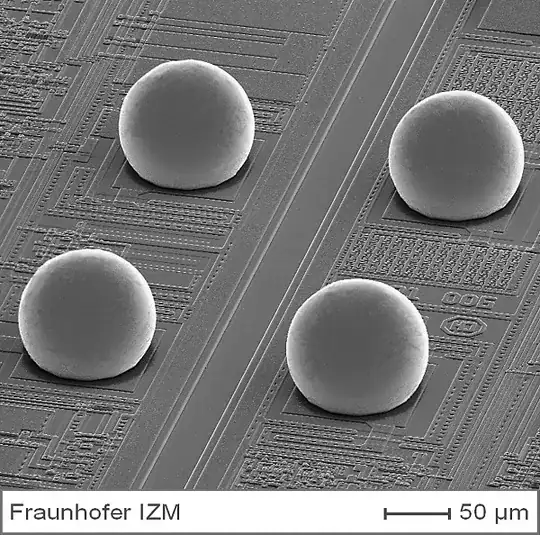
There are indeed larger areas on a die which don't require the 28 nm small size. Typical is the solder ball pads for a flip chip:

enter image description here

Notice the scale: these pads are 1000 times larger than the finest structures on the die. Here a less fine mask may be used, but again, if the process step would also require the 28 nm then the same mask will be used for both. It's not because the pads are gigantic that they don't have to be positioned precisely, and that's less error-prone if you don't have to switch masks.

stevenvh
  • 145,145
  • 21
  • 455
  • 667
  • Lower power consumption? Have you seen the size of my heatsink? – Rocketmagnet Sep 28 '12 at 16:28
  • @Rocket - :-), and yet... smaller gate capacitance menas less energy is pumped from Vdd to ground on each 0-1-0 transition. I don't dare to think of a 1 billion transistor processor at 3 GHz in 1 um technology :-/. (And not just for the 1 square meter package, though it would help in cooling :-)). – stevenvh Sep 28 '12 at 16:39
  • "It's just that the 28 nm mask won't be swapped for a 65 nm mask " is incorrect. Fine features (poly, Gate, Contact) use the finest feature size, but subsequent layers use progressively coarser lithography. It's a cost thing. Scanners/steppers at lower resolution are lower cost and masks are less expensive. – placeholder Sep 28 '12 at 16:43
  • @Tony - I meant there won't be used two different tech masks for the same production step. If your IC needs, say 25 successive steps, they won't use 40 masks for it. (BTW, what are you doing here?) – stevenvh Sep 28 '12 at 17:01
  • @stevenvh - Doesn't small gate size also mean more leakage? I thought that was what contributed to much of the power consumption of a modern CPU? – Rocketmagnet Sep 28 '12 at 17:13
  • @Rocket - No, and I misunderstood this at first too: the capacitance will be charged through a resistance, and you lose the same amount of energy in it as the capacitor will hold. That means the energy only depends on the capacitance, not on the resistance! – stevenvh Sep 28 '12 at 17:22
  • @stevenvh - No, I mean leakage as in [Subthreshold conduction](http://en.wikipedia.org/wiki/Subthreshold_conduction). – Rocketmagnet Sep 28 '12 at 17:35
  • @Rocket - Ah, I see, sorry. That's static power, independent of clock frequency, which you'll also have without clock signal. That will be far less than the power at 3 GHz, though it may/will be more than the same processor if it would have been made in a 1 um process. But that's not the reason for your huge heatsink! :-) – stevenvh Sep 28 '12 at 17:52
  • @Rocket - Come to think of it, it's not fixed: it will increase with temperature, so with frequency, but I don't have figures. – stevenvh Sep 28 '12 at 17:58
  • At very thin GOX the dominant leakage is gate leakage. Tis partially solved by using high-K dielectric in the GOX (HfOx) to have a thicker oxide and not lose gate drive. – placeholder Sep 28 '12 at 18:46
  • @Tony - I wish you would stay away here. Nothing personal, but you and I know you should not be here. Not for a while. – stevenvh Sep 28 '12 at 18:48
  • @stevenvh - According to [this graph](http://chipdesignmag.com/display.php?articleId=261) static power is now greater than dynamic power in some chips. – Rocketmagnet Sep 28 '12 at 19:41
7

"Technology" isn't really the right term for what you're asking. The technology of the chip is determined by the specific processing steps required to make it, and among other things, this determines the minimum feature sizes for various items on the chip. The number commonly associated with a particular technology (e.g., 28 nm) refers specifically to the minimum gate length, which is determined by the width of the lines that can be drawn on the mask that forms the transistor gates.

To be sure, not all transistors on any given chip require the minimum gate length, and many require more than the minimum gate width (for greater current-handling capabiilty), so yes, you will indeed see transistors of many different sizes on a chip.

Dave Tweed
  • 168,369
  • 17
  • 228
  • 393
  • Thanks for your answer. Do you by any chance have any idea of the proportion of transistors that are scaled to the minimum gate size? (Even a rough approximation would be great) Is this done also for cost reasons? And where do the smallest transistors go? (In the cache memory, control unit, or ...) Thank you very much. – user123 Sep 28 '12 at 16:03
  • In a logic process almost all transistors are minimum feature size in gate length. The transistors are designed to yeild best at that length. The transistors that can handle higher voltage are usually place closest to the pads but there typically is no need to have them else where unless there are analog block on chip. – placeholder Sep 28 '12 at 18:44
5

In any given modern process it is very common to have multiple GOX (Gate Oxide) thicknesses. This is not used for cost reasons but for interfacing to the outside world. The core will run at the lowest voltage and on a thinner GOX but will be very much faster. The thicker gate oxide transistors are connected to the package pins, are slower but operate at higher voltages.

As you scale the GOX thickness the physical size of the transistor must also increase.

Adding in additional steps to accomodate this dual GOX flow actually increases cost of the process. But it won't be able to work other wise.

placeholder
  • 29,982
  • 10
  • 63
  • 110
  • But does this change feature size? – Federico Russo Sep 28 '12 at 15:07
  • 2
    Typically the gate masks are always shot with the same photolithography, so technically it is the same features size, because feature size is determined by wavelength, mask techniques and photoresist techniques. However, we use the same litho systems to ensure that the overlay accuracy is the same. But I think you meant to ask are the transistor bigger? Yes, they have to be -> that's what's meant by the "physical size" above. – placeholder Sep 28 '12 at 15:10
1

technology node can be related with feature size ( mim length of the MOS transistor channel b/w the drain and the source). if IC is 28nm, it means mim length channel is 28size not every channel length is same, but same time it does not means that it goes to 65nm.

kakumar9
  • 11
  • 2
  • 1
    This does not appear to answer the question. It might help if you review the original question and existing answers to see what new information can be added. – David Apr 11 '15 at 09:40
1

The reason to use different technologies is to reduced static power (basically leakage current on the transistor). At 90nm process static power starts comparing and eventually overshadow dynamic power. And how it can be implemented, well silicon manufacturing process involves masks and etching if you can do a 28nm procress I would assume a 65nm process could be done using 28nm it would be just a big transistor on the masks

Kvegaoro
  • 3,141
  • 17
  • 14
  • "and eventually overshadow dynamic power". But smaller feature size allows higher clock speeds, so dynamic power increases as well. – Federico Russo Sep 28 '12 at 15:09
  • 1
    http://chipdesignmag.com/display.php?articleId=261 From their charts it shows that dynamic power does increases but not as much as static power does on those small size technology – Kvegaoro Sep 28 '12 at 18:01