Yes, but not as effective as a ground plane. There is capacitance between a conductor (trace) and the reference plane, with a power plane there is added inductance from the power supply. The other problem is slots, as your more likely to have slots in a power plane as a reference plane, slots are bad because they redirect the return current and create more inductance which slows the signals down\higher rise times.
Changing Reference Planes.
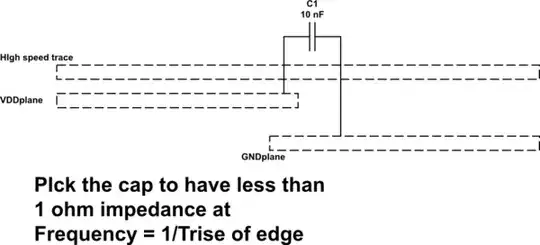
When a signal trace changes from one layer
to another on a PCB, the return current path is interrupted since the
return current must also change reference planes (see right hand
figure below). The question then becomes how does the return current
get from one plane to another? As was the case for the split planes
mentioned above the interplane capacitance is not usually large enough
to be effective, so the return current will have to flow through the
nearest decoupling capacitor in order to change planes. This
obviously increases the loop area and is undesirable for all the
reasons previously stated. One solution to this problem is to avoid
switching reference planes for critical signals (such as clocks), if
at all possible. If you must switch the return path from a power
plane to a ground plane you should place an additional decoupling
capacitor adjacent to the signal via in order to provide a
high-frequency current path between the two planes for the signal
return current. This is not an ideal solution, however, since the
return current must now flow through a via, a trace, a mounting pad, a
capacitor, a mounting pad, a trace, and finally a via to the other
plane. This adds considerable additional inductance in the return
path (typically 5 to 10 nH).
Source: http://www.hottconsultants.com/techtips/pcb-stack-up-6.html