8

Example:
Name?

Does this drawing has a technical name?

I see that people usually call these drawings "PCB". But, PCB is physical object, physical implementation of circuit, isn't it? Is these kind of drawings really called "PCB", or do they have a special name?

hkBattousai
  • 13,913
  • 31
  • 114
  • 190
  • This is merely one of the layers of your PCB. In this case apparently one of the outer layers. You could call it something like "layer x drawing", for example. – Olin Lathrop Sep 26 '12 at 17:30
  • 1
    I would call that one of the perhaps many 'signal layers' of your PCB. Or the signal layer X as suggested by Olin. – kenny Sep 26 '12 at 17:43

6 Answers6

10

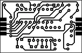
I would also call the drawing you show a "PCB layout", as it obviously isn't the PCB object. But like Wouter already indicated the definition of a PCB contains a lot more information that the copper pattern shown. First, this is just one layer, there could be a second copper pattern on the top/bottom side (for PTH the default copper layer is bottom, for SMT it's top), and inner layers, up to about 20 in the extreme.

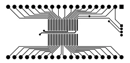
In general you won't find a drawing that includes tracks/pads and drillings, because that's already too much information for one drawing. The drillings drawing will show a series of different markers, like +, x, T, etc, for different hole diameters. Usually you'll have 1 drill drawing, since the hole will go through all layers in most cases. If you have the wallet for it you can have blind or buried vias, and the the drilling will be different for each layer.

My drawings start with the board outline, and that's often a pretty boring drawing, as it can be just a rectangle, but also a more complex outline like this one

enter image description here

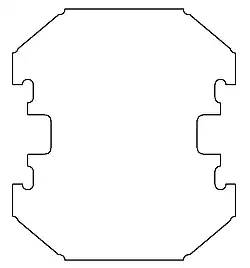
is possible. Each of the component layers will have

  • a copper layer (no distinction is made between tracks and pads)
  • a solder mask layer (which leaves the pads clear)
  • a "silk" layer, containing texts to be printed, like refdes's, logo's and identification
  • a mechanical/keep-out layer, which shows the designer where he shouldn't place components, or indicating how much height he has available in certain areas. (This layer is of no use for the PCB manufacturer.)

So "PCB layout" is only part of the drawings, and in many cases should be called "PCB layout top" or "PCB layout bottom".

stevenvh
  • 145,145
  • 21
  • 455
  • 667
4

The picture you show is the copper side (bottom layer copper) of a PCB. It shows the copper (and the outline). It does not show the drills as such, only the absence of copper that suggests drills at certain places. A real drill picture could for instance also show drills at the corners that are not surrounded by copper.

There are many more layers, for instance in rough order of probability:

  • drills
  • bottom solder screen
  • top silkscreen
  • top copper
  • top solder screen
  • bottom silk screen
  • for more than 2 layers: additional copper and drill layers
Wouter van Ooijen
  • 48,407
  • 1
  • 63
  • 136
3

I think the word you're looking for is Gerber:

The Gerber format is a file format used by printed circuit board (PCB) industry software to describe the images of a printed circuit board (copper layers, solder mask, legend, drill holes, etc.). The Gerber format is the de-facto industry standard for printed circuit board image transfer.

Gerber files are actually ASCII text files:

G75*
G70*
%OFA0B0*%
%FSLAX24Y24*%
%IPPOS*%
%LPD*%
%AMOC8*5,1,8,0,0,1.08239X$1,22.5*%
%ADD10C,0.0080*%
D10*
X000281Y000835D02*
X002472Y006196D01*
M02*

But programs used to view Gerber files create images like this one you've shown and this one:

gerber image

The programs create those images for human consumption. But the ASCII is read just fine by the CAM Machines used to create the PCBs.

From What is a Gerber File?:

In many ways, Gerber is the electronics world's equivalent of PDF. This odd little format, a hybrid machine control language and image, is a core component of the electronics manufacturing supply chain.

embedded.kyle
  • 8,411
  • 2
  • 26
  • 44
  • I disagree: gerber is a format (or collection of formats, if you want to include excellon drill) used to describe a layer (but not the only one). The representation is not the same as what it represents. – Wouter van Ooijen Sep 26 '12 at 21:00
  • 1
    @WoutervanOoijen When I want to look at the traces, pads, and drill of a PCB assembly, I ask for a Gerber. I receive either a file in Gerber format or a stack of paper with drawings that look like those in the OP. Maybe it's a colloquialism. But in the three electronics related jobs I've had, that's what that type of drawing was called. – embedded.kyle Sep 26 '12 at 21:18
  • When I need a datasheet I go looking for a pdf. But that does not make the two the same: pdf is a format, the datasheet is the content. A gerber can describe for instance a stencil cutout, and a PCb can be decribed in a pdf, although both are less common. – Wouter van Ooijen Sep 27 '12 at 07:56
  • @WoutervanOoijen I understand your point. However, the question was, "What do you call the drawing which contains tracks, pads and drilling points of a PCB layer/side?" When I want a drawing that contains that information, I ask for a Gerber and I receive a drawing that looks like the picture in the OP. **I** call that drawing a Gerber and everyone I've said that to in the companies I've worked for understands what I mean. But like I said, it may just be a colloquialism. – embedded.kyle Sep 27 '12 at 14:42
2

I would call it a "[PCB] layout". It's still somewhat a general term, but applies to your picture better than just "PCB".

Armandas
  • 7,845
  • 1
  • 32
  • 56
0

It's called a layout. Or a PCB layout. Or a PCB design. Specifically, it's a copper layer from a design. I don't know what else you would call it.

Jay Carlson
  • 2,819
  • 1
  • 14
  • 21
0

This is an old question, but I'm surprised that nobody mentioned the term artwork. Artwork is the traditional term for the actual graphical pattern to be printed and etched to a circuit board or an integrated circuit.

Nowadays it's old-fashioned and most people simply call it the "PCB layout". But artwork is still a valid, unambiguous term that is recognized by most people in the industry.

For example, an old advertisement in an electronics trade journal (1998) says:

The designer needs to send the CAD data in Gerber format, which is done by rurming the CAD data through a Gerber post processor and outputting the data in Gerber format. A net-list, with drill files usually in Excellon format, will specify the apertures and will be used to drive the NC machines. Drawings or artwork for each layer of the PCB will be used by the photo-tooling machines to expose copper for the tracks. Gerber data is typically provided in vector format, but today raster plotters can rasterize vector data.

I guess the usage of this term declined as most people find that calling a piece of electrical design a work of art is somewhat strange [1], but the word actually has a technical sense. Merrier-Webster Dictionary defines it as...

Artwork: (2)(b) material (such as a drawing or photograph) prepared for reproduction in printed matter.

I think the term originated from the printing industry.

[1] Well, I acknowledge that creating layouts for high-speed, precision, space or layer restricted devices can certainly be an art, but most circuit boards are not that unusual.

比尔盖子
  • 6,064
  • 2
  • 24
  • 51