12

I am trying to reduce the power dissipation of a P-Channel MOSFET high side switch. So my question is:

  • is there any way in which this circuit can be modified so that the P-Channel MOSFET will always be "fully-on" (triode / ohmic mode) no matter what the load is?

Edit 1: Please ignore the on/off mechanism. The question remains somehow the same: how can I always keep V(sd) the smallest possible (P-MOSFET fully on / ohmic mode), independent of the load so that the power dissipation of the MOSFET is minimal.

Edit 2: The switched signal is a DC signal. Basiclly the circuit replaces a switch button.

Edit 3: Voltage switched 30V, max current switched 5A.

enter image description here

Buzai Andras
  • 737
  • 4
  • 10
  • 20
  • 1
    "always" is asking too much, there will always (!) be trnsitory states during switching. Your transistor will do the turning on quickly, but R1 will cause a slow turn off. Better drive both sides actively. There are special chips for this task, like the [these](http://www.microchip.com/ParamChartSearch/chart.aspx?branchID=9010&mid=11&lang=en&pageId=79) – Wouter van Ooijen Sep 24 '12 at 20:55
  • @WoutervanOoijen Yes. You are correct. But please ignore the on/off mechanism. The switching frequency will be extremely low :). Once turned on, the circuit will stay in that state for some time before it will get switched off. Basically it will replace a switch button. Probably it would be more easy to use a chip, but I would not learn much that way :). – Buzai Andras Sep 24 '12 at 21:25
  • It doesn't look that your Vds is dependent on the load. – Szymon Bęczkowski Sep 24 '12 at 22:04
  • Voltage switched= ? Current switched max = ? – Russell McMahon Sep 25 '12 at 02:18
  • 30 V Vgs is too much for most FETs. Consider placing a resistor in series with the collector to form a voltage divider with R1. – stevenvh Sep 25 '12 at 09:55
  • @stevenvh How about using a zener diode to limit/clamp the Vgs voltage? Would that be a good solution? Or the zener will add to much noise or other problems? – Buzai Andras Sep 26 '12 at 15:13
  • @Buzai - No, noise won't be the problem, but a zener needs much more current than a resistor divider. May not be a problem, as the current will only flow when the load is switched on, and then the 10 mA may not matter much. A zener may be a better choice, however, if the input voltage varies a lot, and you always want Vgs as high as possible; with the divider Vgs would decrease if Vcc decreases. – stevenvh Sep 26 '12 at 15:17
  • @stevenvh In the final design the input voltage will be selectable between these values: 10V, 20V and 30V. – Buzai Andras Sep 28 '12 at 12:35
  • @Buzai - In that case I would definitely go for a 15 V zener, a 1/2 divider would only give 5 V gate voltage at 10 V supply, and the FET may not give enough current for *any* load (though a logic level gate FET should give you several amperes at 5 V Vgs). – stevenvh Sep 28 '12 at 12:40
  • @stevenvh I have one more question. For the setup from the image is there a way to speed up the turn-off time of the FET? – Buzai Andras Sep 28 '12 at 19:54

2 Answers2

10

Knowing the voltage being switched and max current would greatly improve available answer quality.

The MOSFETS below give examples of devices which would meet your need at low voltage (say 10-20V) at currents higher than you'd be switching in most cases.

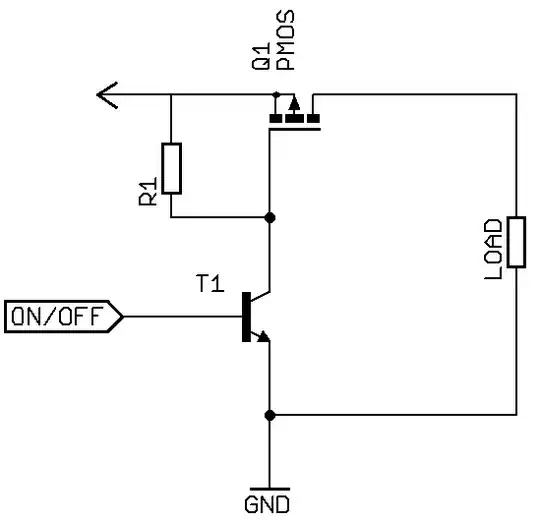
The basic circuit does not need to be modified - use it as is with a suitable FET - as below.


In the steady state on mode the "problem" is easily addressed.

  • A given MOSFET will have a well defined on resistance at a given gate drive voltage. This resistance will change with temperature, but usually by less than 2:1.

  • For a given MOSFET you can usually decrease on resistance by increasing gate drive voltage, up to the maximum allowed for the MOSFET.

  • For a given load current and gate drive voltage you can choose the MOSFET with the lowest on state resistance that you can afford.

  • You can get MOSFETS with Rdson in the 5 to 50 milliohm range at currents of up to say 10A at reasonable cost. You can get similar at up to say 50A at increasing cost.


Examples:

In the absence of good information I'll make some assumptions. These can be improved by providing actual data.

Assume 12V to be switched at 10A. Power = V x I = 120 Watts.
With an Rdson hot of 50 milliohms the power dissipation in the MOSFET will be I^2 x R = 10^2 x 0.05 = 5 Watts = 5/120 or about 4% of the load power.
You would need a heatsink on almost any package.
At 5 milliohms Rdson hot dissipation would be 0.5 Watts. and 0.4% of load power.
A TO220 in still air would handle that OK.
A DPak / TO252 SMD with minimal PCB copper would handle that OK.

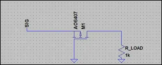
As an example of an SMD MOSFET that would work well.
2.6 milliohms Rdson best case. Say about 5 milliohms in practice. 30V, 60A rated. $1 in volume. Probably a few $ in 1's. You would not ever use the 60A - that's a package limit.
At 10A that's 500 mW dissipation, as above.
Thermal data is a little uncertain but it sounds like 54 C/Watt junction to ambient on a 1" x 1" FR4 PCB steady state.
So about 0.5W x 54 C/W = 27C rise. Say 30C. In an enclosure you'll get a junction temperature of maybe 70-80 degrees. Even in Death Valley in midsummer it should be OK. [Warning: DO NOT shut the door on the toilet at Zabriski Point in mid summer !!!!][Even if you are a woman and the Hell's Angels or similar have just arrived][My wife will tell you about it][But your MOSFET would be OK.]

Datasheet AN821 appended to datasheet - Excellent paper on SO8 thermal issues

For $1.77/1 you get a rather nice TO263 / DPak device.
Datasheet via here includes a mini NDA! Limited by NDA - read it yourself.
30v, 90A, 62 K/W with minimal copper and 40 k/W with a whisper. This is an awesome MOSFET in this type of application.
Under 5 milliohms achievable at many 10's of amps. If you could access the actual die you could possibly start a small car with this as the starter motor switch (spec'd to 360A on graphs) BUT the bondwires are rated at 90A. ie the MOSFET inside greatly exceeds the package capability.
At say 30A power = I^2 x R = 30^2 x 0.003 = 2.7W.
0.003 ohms seems fair after looking at the data sheet.

TimH - Codidact
  • 717
  • 1
  • 6
  • 12
Russell McMahon
  • 147,325
  • 18
  • 210
  • 386
9

The load is not the main issue for keeping the Rds as low as possible, it's the Vgs you need to concentrate on.
For a PMOS the lower the gate voltage, the lower Rds (as Russell points out, higher absolute Vgs). This means in this case the input signals lowest point will cause the highest Rds (if it's an AC signal)

So there are 4 options that come to mind:

  1. Lower the gate voltage (increase absolute Vgs) as much as possible (whilst staying within specs of course)

  2. Raise the DC level of the signal (or reduce the pk-pk swing)

  3. Use a 4-lead MOSFET (so you can bias substrate separately from source) so signal voltage does not affect the Rds.

  4. The obvious one that goes with all the above - use a MOSFET with a very low Vth/Rds

  5. If it is an option, using a second MOSFET in parallel will reduce the total resistance by half, so the power dissipation is halved. This means the power dissipation of each individual MOSFET is 0.25 of the one MOSFET version. This assumes ideal Rds matching ( MOSFETs have positive tempco and components from the same batch will be pretty close so it will be close) This would make a big difference, so may be worth the extra space/cost.

To show how Rds varies with the input signal have a look at this circuit:

MOSFET Rds

Simulation:

MOSFET Rds Simulation

The green trace is the input signal, and the blue trace is the MOSFET Rds. We can see as the input signal voltage drops, Rds rises - very sharply below a Vgs of ~1V (the threshold voltage for this MOSFET is probably around this level)
Note that the voltage only dips a tiny way into the beginning of MOSFET turn-off; this happens very quickly, even another few millivolts would produce considerably higher Rds.

This simulation shows that when the MOSFET is turned on fully, the load should have very little effect:

MOSFET Load Vary Sim

The X axis is the load resistance (R_load) and the blue trace is the MOSFET Rds over the range 1Ω to 10kΩ. We can see Rds varies by less than 1mΩ (I suspect the sharp transitions are just SPICE, but the average value should be reasonably reliable) The gate voltage was 0V and the input voltage was 3VDC.

Oli Glaser
  • 54,990
  • 3
  • 76
  • 147