1

I'm designing a power amplifier and the following circuit is the output stage. My output stage consists of two complementary transistors for both positive and negative waves, but for better understanding, I will only show the one which handles the positive waves.

enter image description here

  • Vcc = 12 V
  • Load = 8 Ω resistor
  • Output current (max) = 1.1 A
  • Output voltage (max) = ~ 8 V
  • IN = sinus with ~8 V amplitude and an extremely low (~250 μA) current as the discrete Darlington needs a low input current.

As far as I know, R1, R3 and R4 and D1 and Q3 are for current and power limitation. How does that work, and how can I calculate these three resistors?

ocrdu
  • 8,705
  • 21
  • 30
  • 42
Markus
  • 21
  • 3
  • You simply choose Rgts II to be If / 0.5V where Vbe starts to conduct Ib and Ic=hFE Ib to pull down input, BUT you must have a series R on input. What is your source voltage and current or Series R? There are better ways – Tony Stewart EE75 Jan 19 '19 at 19:47
  • 1st you must define ALL input + output signal range and source resistance and/or input impedance then tolerances. http://tinyurl.com/ycqwn9l6 expect a 3V drop The rest is Ohm's Law. – Tony Stewart EE75 Jan 19 '19 at 20:39
  • I added all input + outputs – Markus Jan 20 '19 at 13:19
  • Thankyou. Let me assume these are maximum bias currents of say Bass peak at 25Hz while some mid-range like 1Khz is superimposed. Next you MUST define an acceptance criteria or spec, such as THD or IMD and delta T rise. ( assuming all transistors and D1 are at same temp) so that IMD is limited to variation in hFE due to **Ib(max/min) current & ΔT** only regardless of max or min hFE, just the ratio. R2 will also affect BW but more important is THD before gain feedback reduction, which I may later assume is 10 to 100 unless that is fixed. – Tony Stewart EE75 Jan 20 '19 at 17:11
  • Thank you but for now, I'm more interested in the resistors R3 & R4 as they are for current and power limitation and I don't really understand how it works and how I calculate them. May you help me with that? – Markus Jan 20 '19 at 17:19
  • Again, what is your expected acceptance criteria? – Tony Stewart EE75 Jan 20 '19 at 17:38
  • This is not important. I'm not gonna use it, it's just for learning purpose. I don't have any special criteria. It just should be as linear as possible. – Markus Jan 20 '19 at 17:55
  • You must learn what matters e.g. cost, reliability , performance {efficiency, THD,IHD, dynamic range, SNR} when analyzing any design, In this case excess bias current is needed to keep Imax/Imin within a 10:1 to 100:1 range so hFE variation is small and not say hFE from 10 to 300 due to Imax/min and T rise. It is better to have low hFE and smaller variation than high hFE with big percent variation – Tony Stewart EE75 Jan 20 '19 at 18:06
  • then learn that speakers are helmoltz resonator magnetic RLC equiv cct. not 8 Ohms but a dozen RLC parts, then you will understand why performance varies. and linearity and dampening factor or relative load to driver ratio – Tony Stewart EE75 Jan 20 '19 at 18:14
  • If you want high linearity and high efficiency then a current source is needed for bias. or active regulated bias.so Q1 is never starved in +ve cycle. for crossover distortion and hFE modulation – Tony Stewart EE75 Jan 20 '19 at 18:49

3 Answers3

1

The first thing to do is to redraw the schematic into a somewhat better (more readable) layout. (You can read a short discussion I wrote here.)

schematic

simulate this circuit – Schematic created using CircuitLab

(I've changed the designations for the parts, above. Live with it. The schematic editor labels them for me and I'm not going through the trouble to rename them. I think you can still follow along okay.)

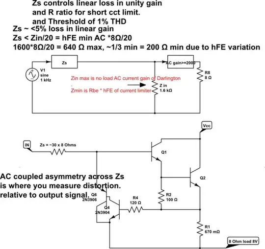
The above circuit is one quadrant of a two quadrant output driver. This quadrant can source current into the load but cannot sink current from the load. So you'll need a second quadrant to provide the sinking capability. Obviously, this is one half of a two-quadrant output driver stage. (A motor driver requiring both power delivery to the motor and absorbing power from braking, both forward and backward, would probably need a four-quadrant system. In this case, there is only power delivery to the load and no expectation of absorbing significant power from the load, which isn't expected to be a significant source of power back into the circuit.)

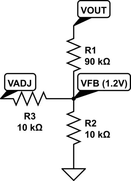
There's already a great answer regarding \$R_2\$ (as in the schematic above) found at EESE: resistors within a Darlington transistor. That explanation should help a great deal, I think. Feel free to ask additional questions you feel aren't answered there. But that answer is pretty easy to follow, I think. As you should be able to work out from reading it, there's no "bright line" about creating a specific value for \$R_2\$. It will be a matter of the parts you select, your goals in the circuit, and your judgment and experience.

Different engineers would likely select somewhat different values for \$R_2\$ and would be able to make good arguments for their choices. Perhaps the most important thing is merely that you actually have a defensible argument for your choice and that you didn't simply choose a value without any thought at all. You should be able to explain why you chose what you chose. That's all.

\$R_1\$ exists for several reasons. It's important, for example, even if \$Q_3\$, \$D_1\$, \$R_3\$, and \$R_4\$ didn't exist to more sharply curtail (limit) output current. By itself, the voltage drop across \$R_1\$ as output current increases will tend to push upward on the Darlington emitter, pinching its base-emitter drive voltage and acting to help limit the output current and power dissipation in the Darlington parts in the case of a shorted output.

But \$R_1\$'s voltage drop here also provides a signal that is fed back to the base of \$Q_3\$ via \$R_4\$. At some point, the voltage drop across \$R_1\$ caused by the load current will reach a voltage value that, less a slight drop across \$R_4\$ when supplying base current into \$Q_3\$, will cause \$Q_3\$'s collector to start pulling current away from the base of \$Q_1\$. As it does so, the Darlington becomes starved of drive current, limiting the output current more sharply than before because there is now a circuit actively working to remove drive at the source (the base of the Darlington) as well as merely passively pushing upward on the Darlington emitter.

Of course, this would be useless if the signal at IN were a low-impedance voltage source. In that case, all that would happen is that \$Q_3\$ would simply pull lots more current heading towards the load, bypassing the rest of the circuit (and \$R_1\$, as well.) And that's the opposite of what would be desired. The only way this works is when the drive (IN) voltage drops when \$Q_3\$ pulls current away, diverting it towards the load to bypass the Darlington. This means there needs to be significant source impedance present, driving this quadrant. Otherwise, \$Q_3\$ (and supporting parts) don't work as intended.

(Since a Darlington often only requires a modest current compliance for its drive, diverting a significant part of it away via \$Q_3\$ should not damage the load. For example, if the circuit were arranged so that the Darlington could supply up to \$1\:\text{A}\$ maximum and only required \$1\:\text{mA}\$ of base drive compliance to achieve that, then if \$Q_3\$ diverted all of the \$1\:\text{mA}\$ away from the Darlington and into the load (designed to handle up to \$1\:\text{A}\$), you can see that the load could easily handle the diversion without trouble. Meanwhile, the Darlington is completely turned off and could no longer supply that \$1\:\text{A}\$ to the load.)

jonk
  • 77,059
  • 6
  • 73
  • 185
  • @Hearth Thanks so much for the catch. Appreciated! – jonk Jan 20 '19 at 02:49
  • @jonk thank you very much! I'm just still wondering what exactly R4 & R3 does as the current limitation would also work without them. – Markus Jan 20 '19 at 09:12
  • @Markus Try read this http://hifisonix.com/wordpress/wp-content/uploads/2013/05/soaprot_12-03-2012.pdf – G36 Jan 20 '19 at 10:49
  • @G36 I still don't get it. I updated all the input & output values. If someone could tell me how to calculate R3 & R4 & R1 it would be awesome. – Markus Jan 20 '19 at 13:57
  • @Markus We can tell you a few ways to consider how, but there is no bright line "right way always" to do that. I'd have to write about all the various possible tradeoffs to consider, why A might be better in circumstance 1, but where B might be better in circumstance 2, etc. You need to spend some time understanding this circuit in three stages: (1) Just \$Q_2\$ and \$R_1\$; and, (2) Adding in \$Q_1\$ and \$R_2\$; and, (3) Adding in the rest (though you don't actually need \$D_1\$ you could also try and work out why you may or may not want it.) I don't want to rewrite already existing books. – jonk Jan 20 '19 at 20:05
0

I'm more interested in the resistors R3 & R4 as they are for current and power limitation and I don't really understand how it works and how I calculate them.

For Power Amps the main design tradeoffs are heat rise and non-linearity at current range. The hFE is a critical factor as it can vary 10:1 over a very wide range of currents as well as Vce & T rise. It is also interesting to know that BJT's perform better hot and MOSFET's perform better cold. But the current limiter here is to prevent Q2 from burning up from a short circuit fault.

In order to detect current Vbe sense the voltage drop across Re so to regulate this limit, with proportional feedback (PID theory) the limit error is inversely related to the loop gain and drift in the voltage reference.

Since R3/(R3+R4) ratio forms a feedback attenuator, that reduces loop gain and increases error. For optimal heat protection, you want R4=0 to increase the current loop gain and reduce the limit error above your Current limit setpoint of Vbe/Re = 1A, then R3 is redundant.

Yet, BackEMF is stored load energy. So the L/R or ESR*C of an overcurrent load must be defined or at least considered, like a pumpmotor or a supercap being charged or a woofer being connected. Thus R4 can be useful for Q3-Ib protection but R3 makes current limiting softer and is just a loop gain attenuator. So you must decide between Thermal margin and compression distortion while limiting current. This has been the basis for another class of design with current booster transistors added to the basic Class A-B design.

Recommendation

Let R4 = 12V/100mA ~ 120 Ohms where I want Q3-Ib to handle a 100mA transient. Then do not install R3.

schematic

simulate this circuit – Schematic created using CircuitLab

Caveat

Since Re senses current limit it also attenuates the signal 0.4/8ohms = 5% So I am speaking about additional attenuation from Zs/Zin ratio to provide linear gain and current limiting. There are many details not discussed.

enter image description here

Tony Stewart EE75
  • 1
  • 3
  • 54
  • 182
  • Note that it is hard to see TP2 asymmetry difference ratio of 0.01/4.63=0.2% distortion but across Zs you can see it easily then TP3 base current and collector current feedback starting to attenuate the input. The 10Meg is just a scope probe AC coupled. View here http://tinyurl.com/yapxovng – Tony Stewart EE75 Jan 21 '19 at 00:31
0

Q3 and the associated components are to provide protection for the output transistors in case of overload.

The basic circuit would not require R3 and R4 with the base of Q3 directly connected to resistor R1.

R1 provides current sensing with the voltage across it being proportional to the current flowing into the load (and the output transistor Q2).

When the voltage across R1 reaches ~600mV Q3 starts to conduct and diverts base current away from Q1 (and Q2) to prevent the current form increasing. This provides some protection but the power in Q2 can still reach high levels as it can a high voltage across it at the same time as high-current, if for example the load is very low resistance (such as a short-circuit).

R3 and R4 provide additional protection in that when the output voltage is low, there will voltage across R4 will be added to that across R1 so that a lower current is required for the current-limiting to come into effect. For example if there is 300mV across R4 when the output voltage is low it will only require an additional 300mV across R1 for protection to start, this would reduce the power dissipated in Q1 under such conditions by a factor of 2.

As the voltage at the output increases (and gets closer to Vcc) the voltage across R4 reduces until with the output at Vcc there would be no additional voltage.

This technique is often referred to as foldback protection and is common in power supplies but can be difficult to use in audio power amplifiers where the load may have an inductive component. This can require that the amplifier output high-currents while at low voltage causing the protection to come into effect and resulting in distortion.

In power supplies similar difficulties can occur with turning on a load, the protection can make it difficult to start powering a load with large capacitors or one that takes a high-current to start, such as motors.

The result is that the choice of values for R3 and R4 is usually a compromise and too much foldback can reduce the performance of the amplifier or power-supply.

Wikipedia - Foldback Current Limiting

Kevin White
  • 32,097
  • 1
  • 47
  • 74