8

I've done a preliminary layout of my crystals. I've never designed a board with crystals so this is just a rough first pass based on my small set of working knowledge of crystal layout. How am I looking so far? Anything I could be doing better?

Details on the board:

  • 4 layer (from the top: signal - ground - split power planes - signal)
  • Y1 is 32.768KHz
  • Y2 is 12MHz
  • load caps are 15pF and 18pF for Y1 and Y2 respectively
  • for scale, the space between Y2's pads and the MCU keepout is 1.75mm

Note: this picture doesn't show the MCU power/ground pins. I have them all bypassed with a bevy of 0.001uF, 0.01uF and 0.1uF ceramics on the outside perimeter of the MCU with direct connections to the 3V3 power plane and ground plane through short traces to vias under the chip

EDIT: Updated the crystal layout and picture. I pulled in the crystals towards the MCU and pulled in the load capacitors to the crystals. Even though I'm told it's not important, traces are nearly equal from crystal to MCU. The traces for Y2 are only off by 4 mils if my math is correct. :D
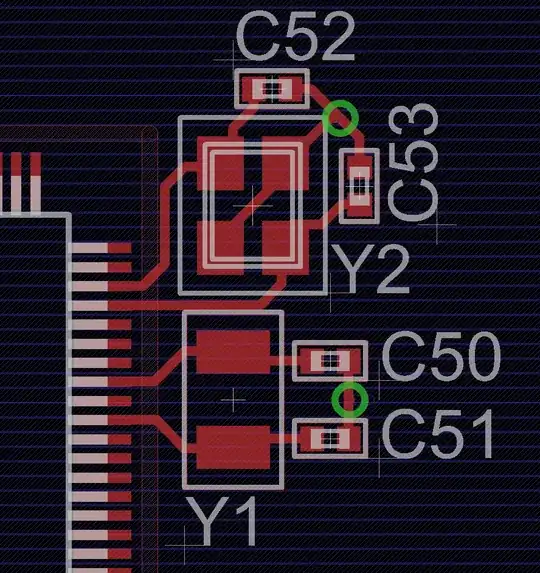
crystal layout

Toby Lawrence
  • 3,098
  • 2
  • 26
  • 34
  • Looks OK, but you still leave *lots* of space between the components. C50 and C51 for instance can be placed a full mm closer together, and both crystals closer to the controller. And why did you go in a right angle from C52 to C53? I would cut that corner, and place the via so that it nearly touches the crystal's pad. – stevenvh Sep 19 '12 at 12:50
  • Fixed this - updated the picture of the layout. :) – Toby Lawrence Sep 19 '12 at 13:22
  • 1
    An aside: your vias seem dangerously large, somebody might fall into them :-). Are they 1 mm diameter? I usually work with 0.35 mm vias. – stevenvh Sep 19 '12 at 13:33
  • 0.81mm diameter, 0.6mm drill. I just go with whatever Eagle wants to throw me. Rather have big vias and potentially avoid a drill mishit. I haven't had layout problems yet where I'd consider shrinking them to make something work. – Toby Lawrence Sep 19 '12 at 13:55
  • Ah, maybe that's what makes them look so large. The 0.81 mm is the annular ring diameter, right? Then you only have 0.1 mm margin. My 0.35 mm vias have a 0.75 mm annular ring, so that's twice as wide. – stevenvh Sep 19 '12 at 15:21
  • Right, 0.81mm is the annular ring. Funny thing is... they're still like ballpoint pen dots, more or less, in person. :) – Toby Lawrence Sep 19 '12 at 16:17
  • let us [continue this discussion in chat](http://chat.stackexchange.com/rooms/5875/discussion-between-toby-lawrence-and-stevenvh) – Toby Lawrence Sep 19 '12 at 17:28
  • Is that an LPC176x? – starblue Sep 20 '12 at 18:05
  • Good eye - yep! I've been working with the LPC1769 base board from Embedded Artists and I'm really enjoying LPCXpresso. Everything has been going fairly swimmingly. It's getting time to start laying out my own board, though, otherwise I'm gonna have like 10 separate building block prototype PCBs all plugged into my breadboard. :) – Toby Lawrence Sep 20 '12 at 18:10

1 Answers1

4

Ideally you want traces from MCU to crystal and from crystal to load caps to be as short as possible and as equal length as possible - in this regard your setup is not ideal, but for such low frequencies my guess you will be OK.

Once i've had lots of problems trying to make MC3PHAC to work as it is very picky regarding to crystal, my traces were of different length and quite long. After trying a horde of different load cap values, ended up using the ceramic resonator that was specified in a reference design.

miceuz
  • 5,523
  • 3
  • 39
  • 49
  • Yeah- I simply picked the particular part for Y2 at random from a page of crystals matching my desired criteria... more just to get something down on the board to fiddle with. I definitely thought about the unequal lengths due to their pin assignments. Maybe I'll take another pick to get something that is two terminal so I can try and equalize the trace lengths better. – Toby Lawrence Sep 19 '12 at 12:53
  • Equal length is *absolutely* overkill for a 12 MHz crystal, where your wavelength is 25 m! For 32 kHz it even becomes ridiculous :-) (wavelength: 10 km). Besides, the signal makes a loop to the crystal and back, it's not like two signals parallel which have to arrive at the same time. – stevenvh Sep 19 '12 at 12:58
  • 1
    If nothing else, equal lengths would make me feel happier when staring at the board on my screen for hours on end. :P (woo symmetry OCD) – Toby Lawrence Sep 19 '12 at 13:03
  • @TobyLawrence: Curious, which crystal exactly is Y2 ? I have a need for a small-footprint SMD crystal as well – boardbite Sep 19 '12 at 14:17
  • Y2 is an ABM8G series from ABRACON. 3.2mm x 2.5m x 1.0mm. Here's a datasheet: http://www.abracon.com/Resonators/ABM8G.pdf. They are $1.17 - $1.35 a piece at Mouser.. so not terribly expensive given their small footprint. – Toby Lawrence Sep 19 '12 at 14:49