I'm working on a project for University. The goal is to create an ultrasonic flaw detector that can measure flaws within a piece of metal. I have only taken introductory courses in the different branches of electrical engineering such as Circuits, Network Analysis, and Electrical Devices. Since my career path is currently in the software industry I haven't been focusing heavily on learning the topics I need to complete this project. Despite that, I've made some progress that I'm happy with.
Here is my current schematic:
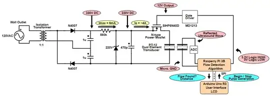
The PT-12 has a resonant frequency of 5MHz, and operates best at a pulse amplitude of 220V. It is a dual-element transducer, meaning that the output and inputs of the transducer run on different cables, and both elements within the transducer are separated by an acoustic barrier.
Since the RF is 5MHz, that gives us a cycle time of 200ns. I've learned that the way these transducers typically operate is through a high voltage pulse of 1/2 cycle or less. This is referred to as pinging the device. So the goal of the pulse generation circuit is to provide a 100ns pulse at 220V amplitude.
My progress was going fairly well until I began thinking about how I'd be switching the pulse on and off again. I thought I could use a simple spst switch at first, and quickly realized that I was deluding myself. It seems that the only solution I could find was using a Power Mosfet.
I researched many different potential devices, as well as the parameters on the datasheets that would be the most important. I found that in order to get as close to 100ns pulse width as possible, I'd need to minimize both the Gate Charges (Qg,Qgs,Qgd) and Delay Times (tf,tr,td(on),td(off)). One potential device I found was SiHP6N40D, http://www.vishay.com/docs/91498/sihp6n40d.pdf.
Which had the following parameters:
It also specifies Rds(on) = 0.85 to 1 ohms. I learned while researching these power mosfets that Rds(on) typically decreases when more cells are added, which in turn increases capacitance and lowers response time. So a good Rds(on) value is near 1ohm for high switching purposes.
I found this equation on the following electronics.stackexchange post. $$ f_{max} = \frac{1}{t_d + t_r + t_f + t_s} $$
And this seems to give 22.22MHz as the switching frequency, however the datasheet does not specify storage time. I'm hoping this parameter was just factored into the other delays. There was another time parameter, trr or Reverse Recovery time, but I'm unsure if this would affect the switching frequency. Assuming it can reach 22.22MHz, that seems to be quite good as it could turn on in 22.5ns and off in 22.5ns.
The next step was to interface the switch with my microcontroller so it could control the sampling rate. I realized the gpio output wouldn't be high enough to meet the Vgs of 10V, and additionally it would be too dangerous to directly connect my Raspberry Pi gpio pins to the power mosfet due to capacitance leakage through the gate. The solution for this was to use a gate driver, which in turn has its own delay times.
I researched some potential gate drivers and found 2 that had very low delay times:
ISL55110 --> https://www.mouser.com/datasheet/2/698/isl55110-11-1302115.pdf
MD1213DB1 --> http://ww1.microchip.com/downloads/en/DeviceDoc/20005713B.pdf
And it was at this point that I reached a threshold of confusion that I felt I needed to get help with. I don't know how to achieve my goal of a 100ns pulse width since there are so many factors to consider: mosfet delay, gate delay, microcontroller toggle speed. And ontop of that, I'm fairly certain now that in order to activate the mosfet gate, Vgs = 10V does not mean 10V is applied to the gate, it means that I would need to apply 230V. Applying only ~10V would put the mosfet into forward bias as according to this post.
In summary, I'd like help with figuring out how to go about approaching this to ensure I get as close to 100ns as I can. Also, if there are obvious problems that I haven't mentioned please inform me of those. Ultimately, if it isn't possible to get near 100ns, I'd be okay with simply being able to send A pulse to the transducer.
Component Calculations:
I've chosen to go with a sample rate of 2kHz, and used that to determine the components in my circuit schematic.
Since the capacitor should be almost fully discharged in 4 time constants (~98%), and I want the pulse to be 100ns
τ = 25ns.
C = 25ns/(50ohms + 1ohm) = ~490pF --> 470pF
*Where 50ohms is the impedance of the transducer and 1ohm is the Rds(on) resistance of the mosfet.
We'd want the capacitor to be charged in less than 1/2 of a cycle of the sample rate, or 250us.
R = 250us/470pF = 530kohm --> 560kohm
The current leaving the capacitor upon switching of the mosfet starts off high
Vc(1ns) = 220V x e^-(1ns/(470pF x 50.32ohm)) = 210.89V
dV/dT = (220V - 210.89V)/1ns = 9.11E9
ic(1ns) = 470pF x 9.11E9 = 4.28A
At the end of the desired time the mosfet should be open, ic would be
Vc(100ns) = 3.2V
dV/dT = (220V - 3.2V)/100ns = 2.168E9 V/s
ic(100ns) = 470pF x 2.168E9 = 1.02A
Extra info:
Why do I have both an Arduino and Raspberry Pi?
I began the semester with the intention of using the Arduino because it had analog input pins already on the board. I had already developed a GUI on an LCD screen I had, when I realized the 16MHz clockrate of the Arduino was not fast enough to control the mosfet switch speed of 100ns. I decided it would be too much work to rewrite the interface in Python. I simply added some code to communicate with the Pi serially which would then send the logic signals instead.
To determine distance, the Pi will simply count the number of clock cycles since the most recent HIGH output on its gate driver pin. Hopefully I'd know what the full delay of the circuitry would be by then, and then this could be factored out of the response time to get the true amount of time the wave took to travel across the measured medium. Specifically, the speed of sound in aluminum is 6320m/s (google). The dimensions of my measured object are fixed at 20cm x 20cm x 2.5cm. So if no flaw is present, the wave would travel the full distance and take 63.2us, otherwise a reflected wave would arrive back to the transducer quicker than that. It's a given that the defect upon testing will be near the middle somewhere, so roughly 31.6us travel time if a defect is present.