17

I am developing a PCB for an analogue sensing application. It uses the internal ADC on a PSoC3. As usual, the application is very space constrained (11mm x 21mm), so I have had to make some compromises in the PCB layout which I would not have done on a larger PCB.

PSoC PCB

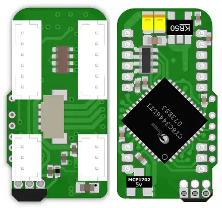
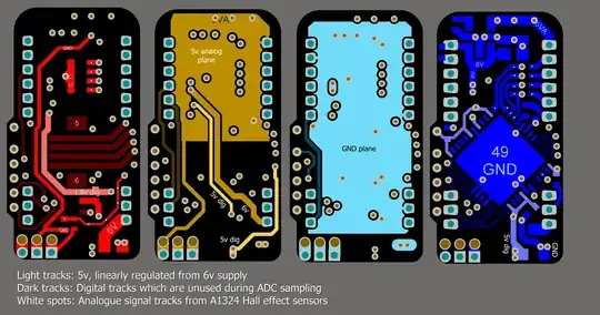
The board is supplied by regulated 6v, and contains two 5v linear regulators. An MCP1702 for the digital supply, and an MIC5205 for the analogue supply. The board is sensing five A1324 Hall effect sensors. Each Hall effect output signal is filtered by a 100nF + 1k RC filter. One sensor is on the PCB itself (bottom right). The other 4 plug into the right hand 6-pin connector.

The chip is acting as an SPI slave, but ADC samples are always taken between SPI transactions, so the SPI should not interfere with the analogue signals.

Sadly, I am still seeing some noise (about 1.5 LSB at 12-bits) on the analogue signals, and I wonder if there is anything I could have done differently in the layout to improve it.

PSoC Layout

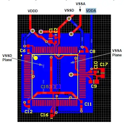
Please open the image in a new tab to see it in higher resolution.


Added:

Other PCB designs I have done using the MCP3208, and the same dual 5v supplies, same sensors, and same RC filters have achieved no noticeable noise at 12 bits.

The ADC on the PSoC3 is a delta sigma type. This version of the PSoC is limited to 12 bits, but another part number has a 16-bit ADC (although with a lower sample rate).

I do care about the noise, and would really like to push it a bit further towards 12 ENOB. The reason is not accuracy, but velocity measurement. Currently this level of noise is making it impossible to do accurate position and velocity control on a robot.


Added:

Schematic. Sorry it's a bit cramped, but you can just about read the values.

PSoC Schematic

Rocketmagnet
  • 26,933
  • 17
  • 92
  • 177
  • Do you mean MCP3208?? That has a 72dB SINAD, or ENOB=11.7 – Scott Seidman Sep 13 '12 at 19:05
  • Whoops. Yes. Corrected. – Rocketmagnet Sep 13 '12 at 20:31
  • Forgot to ask: can you post a schematic? – stevenvh Sep 14 '12 at 08:22
  • @stevenvh - Added. – Rocketmagnet Sep 14 '12 at 14:37
  • Please, please, please stop drawing your schematic entities to look like the physical chip. The whole point of the schematic is to define the *function* of the circuit **visually**. By drawing your schematic like the physical chip layout, you're basically preventing that from happening with any success. – Connor Wolf Sep 15 '12 at 03:40
  • 1
    Also, **STOP USING NET-LABELS!** Your circuit is *nowhere near* complex enough to require them, and by not actually showing the connections, you make it much more difficult to trace connections out. Again, the purpose of the schematic is to make the *intended function and functionality* of the circuit **visually apparent**. You then let the computer translate the visual representation to the actual physical layout of the devices (which is something computers are very good at). – Connor Wolf Sep 15 '12 at 03:42
  • Other complaints would be that you have a lot of sideways ground and power ports. Try to put them vertically (it makes them easier to distinguish visually). By fixing your schematic entities, you should be able to put them all vertically without issue. It's just the weird schematic entity layout that's forcing you to put them sideways to make things fit. – Connor Wolf Sep 15 '12 at 03:45
  • @FakeName - I agree with your comments regarding schematic layout. And I actually do all of those things for some schematics, and I would recommend them to other people too, *unless* they are laying out a desperately space constrained PCB like this one. In that case, the advice begins to work against you. If space is your #1 constraint, then your workflow is different, and the way you use a schematic is different. – Rocketmagnet Sep 15 '12 at 09:27
  • Normally, when you prototype a circuit, you might design a nice big one to see if it works, and help debug it. But when space is the #1 constraint, your prototype is the real size to see if it's even possible. – Rocketmagnet Sep 15 '12 at 09:30
  • I actually find net labels very helpful, and they make the schematic easier for me to read and edit. The board layout constrains which signals can get to which pins, and I often have to move things around to get it all to fit. Disconnecting and reconnecting loads of wires is considerably more of a PITA than moving the labels. – Rocketmagnet Sep 15 '12 at 09:34
  • 1
    @Rocketmagnet - They certainly are helpful *for the person drawing the circuit*. **They're utterly abominable for everyone else**. – Connor Wolf Sep 16 '12 at 07:21
  • 1
    Also, if you are having issues with needing to route wires due to space-constraints, you *desperately* need to look into the [*pin-swapping*](http://wiki.altium.com/display/ADOH/Pin,+Differential+Pair+and+Sub-Part+Swapping) functions in Altium. Basically, you can specify pins that are functionally-swappable in the component definition (I.E. various IO pins), and then when you are routing the PCB, you can run the traces to any of the pins that would work, rather then just the *one* you specified in the schematic. Then, you can synchronize the routing you chose in the PCB to the schematic. – Connor Wolf Sep 16 '12 at 07:25
  • 1
    Basically net-labels are like `goto` in schematic form. They make *your* job a bit easier, but they make anyone else who has to work on or read your schematic's life a lot harder. – Connor Wolf Sep 16 '12 at 07:29
  • Last, are you aware of `ctrl`+drag? It moves component parts while maintaining the connections (schematic editor only). It doesn't always work, but it's very useful. – Connor Wolf Sep 16 '12 at 07:31
  • 1
    @FakeName, while connecting with labels might make it harder to follow a circuit, redrawing every symbol to make a pure & clean schematic with nice straight lines could easily quadruple the time to do schematic entry. I'd love to see a perfect schematic, I'm not sure its realistic to demand one. – The Photon Sep 25 '12 at 18:45
  • 2
    @Rocketmagnet, Having a very small pcb area doesn't mean you can't draw your schematic on D-size paper. – The Photon Sep 25 '12 at 18:46
  • @ThePhoton - You only have to redraw the symbol for each device once. Then you just put it in your component library. – Connor Wolf Sep 25 '12 at 19:02
  • And I do draw schematics as much to the specifications I ask others as possible. I actually don't use net labels. **At all**. It does take a tiny bit more time, but that time is easy saved and more when discussing the designs with other people. – Connor Wolf Sep 25 '12 at 19:04
  • Again, the use of net-labels is very much like `goto`. It may save **you** time, but if you work with other people (and I actually work very closely with another engineer myself), they are an utter, utter time-sink, since every time you're discussing anything, you have to manually go over the entire schematic trying to find where it goes. – Connor Wolf Sep 25 '12 at 19:05
  • @FakeName - Sorry, I'm just going to have to disagree with you there. I'm glad you have an opinion. – Rocketmagnet Sep 25 '12 at 19:53
  • @FakeName, in Altium, it's very nice to use net labels, even if your schematic is fully connected graphically, because then when you get to the layout you get labels on the tracks that remind you the function of each net. – The Photon Sep 25 '12 at 20:13
  • @ThePhoton - Well, I do use them to name wires, but I don't use them to make connections at all. – Connor Wolf Sep 25 '12 at 20:32
  • @Rocketmagnet - If you start working closely with other people on the same design, you'll probably change your mind. – Connor Wolf Sep 25 '12 at 20:32
  • To be clear, I'm not saying that you should *never* use net-lables, just that you should have a **good reason** when you do. Treat them like any other powerful, control-flow modifying programming trick. They remove the visual immediacy of circuit function that a schematic is *supposed* to provide. You don't want to use them unless you have a real good reason to, and if you're not sure you have a good reason, you don't. – Connor Wolf Sep 25 '12 at 20:41

2 Answers2

14

You'll always have some noise on an ADC, especially SA (Successive Approximation) types on the microcontroller die. Sigma-delta perform better for Gaussian noise, as they integrate it. Don't expect 12 ENOB from a 12-bit ADC.

The controller's noise is a reason why most microcontrollers don't give you a higher resolution than 10 bit, and the AVR offers the possibility to stop the microcontroller during the ADC's acquisition, which should confirm that at least some of the noise comes from the controller.

But the question is: do you care? 1.5 bit of noise on a 12-bit ADC still leaves you more than 10 bits, or better than 0.1 %. How accurate is your Hall sensor? Other components in the circuit?

edit
You seem to use the PSoC's internal oscillator, since I don't see any crystal on the schematic. It looks OK: you have the proper decoupling. Apart from the internal clock the only high speed part in the circuit seems to be the SPI, but you say that this will be silent during measurements. The rest of the board is DC or probably relatively low frequent like the Hall effect sensors. And it's a Damn Small™, which also helps: shorter traces will pick up less noise. Sure I could nitpick about the MCP1702, which I would rotate 90° CCW so that the output capacitor can be placed even closer to the pins, but that won't solve the problems.

I only see one change in the layout which might improve your S/N ratio:

enter image description here

In the datasheet split analog and digital ground planes are suggested for "Optimal Analog Performance" (page 10).

For the rest: it's a small board like I said, that means short traces and decoupling within a few mm. So I would like to have another look at the noise's source. Prime suspect is the PSoC's clock. The PSoC can run a very low supply voltage, and that would reduce its noise. Of course it would help much if VDDA has to be lowered as well, but I didn't read anywhere in the datasheet that VDDA shouldn't be higher than VDDD.

Next, the ADC. On page 55 of the datasheet it says 66 dB SINAD, that's 11 bits, close to what you get now. The A1324 datasheet gives us 7 mVpp noise on a quiescent voltage of 2.5 V. That's also far less than the 72 dB S/N ratio which 12-bit could give you. You may improve this a little bit with extra filtering.

You mention the better performance of the MCP3208, but that's an ADC away from the microcontroller, and that may explain how an SA ADC can do better than a sigma-delta with the same resolution.

So, the options I see: lower the digital power supply voltage and split analog and digital grounds.

stevenvh
  • 145,145
  • 21
  • 455
  • 667
  • That is a very interesting idea about lowering the PSoC's digital supply voltage. VDDA certainly can be higher than VDDD. – Rocketmagnet Sep 14 '12 at 19:21
  • So, do you think I should disconnect VSSA from the thermal pad? I have actually posted this as a whole [new question](http://electronics.stackexchange.com/questions/40352/how-to-split-analog-and-digital-gnd-planes-for-a-tqfn-device). – Rocketmagnet Sep 14 '12 at 19:41
2

I agree with the above. 1.5LSB of noise is pretty reasonable. http://www.cypress.com/?docID=39346 shows a minimum SINAD of 66 dB in 12 bit mode, suggesting ENOB = 10.7.

I know this isn't a direct answer to your question, but I'm going to interpret the question as "how do I fix my problems with velocity control?" and not "How do I get more than 10.5 ENOB?".

How are you differentiating? Do you have enough spare clock ticks to do something a hair smoother than a two-point central difference? Maybe work out something 5 samples wide, optimized in Matlab?

Also, this might sound a bit funny, but velocity noise gets worse as you sample faster

$$\frac{1LSB}{\Delta t}$$ gets bigger as delta t gets smaller). Try sampling only as fast as you need to, not as fast as you can.

Not to be insulting, but also take a quick glance to make sure nothing silly is going on in your velocity control, like issues with conversions between signed and unsigned integers, and make sure that your integers are wide enough to avoid overflow errors when you differentiate. My own control equations often get complicated enough that I sometimes explicitly cast each operation.

Lastly, though perhaps most likely, are you losing effective bits off the top by not amplifying to near full scale? If so, you can amplify or perhaps provide a smaller Vref.

Scott Seidman
  • 29,274
  • 4
  • 44
  • 109
  • We are calculating position and velocity using an [Alpha Beta Filter](http://en.wikipedia.org/wiki/Alpha_beta_filter). I understand that velocity noise increases as sample rate increases if done naively. I am sure that velocity noise is not due to a sign error. And we are already almost at full scale, so there is no more amplification I can do without risking hitting the top or bottom of the range. – Rocketmagnet Sep 13 '12 at 08:06
  • Would you say that there are no improvements I can make to the layout? – Rocketmagnet Sep 13 '12 at 08:07
  • Can't see anything yet. How are you amplifying the hall sensors? Have you actually looked at the output of the A-B filters and control eqns as a reality check? Peeked at noise on your regulator outs? It might be illuminating to do a formal noise budget for the whole system – Scott Seidman Sep 13 '12 at 11:14
  • @Halls have no amplification. They already have a 0v - 5v swing. There is no buffering other than the filter capacitor. Have yet to measure the regulator noise, but I do know that this regulator+Hall+Filter has achieved 12 ENOB in another system. We have spent the last month studying the signals, noise and filters. I am very sure they are working correctly. – Rocketmagnet Sep 13 '12 at 11:24
  • It looks like the Cypress sigma delta ADC has a differential mode. Have you tried that? http://www.cypress.com/?docID=39346 seems to say (pg 17) that you might gain a few dB by bypassing the internal Vref. Bottom line, though is that the minimum SINAD of this ADC is only 66dB in 12bit mode, which is pretty close to where you are ((66-1.76)/6.02) gives ENOB=10.67 (But verify that my calcs are right and that I'm looking at the docs for the ADC you're currently using!) I think your choices are different ADC, same ADC more bits, or control algorithm more robust in noise. – Scott Seidman Sep 13 '12 at 17:07
  • Annoyingly the differential mode only gives me a voltage swing of 0v .. 4.096v, so I can't use it. I might try to attenuate the signals in the next version of the board so I can take advantage of this. However, when I tried it, the noise was fractionally worse (probably due to the reduced range). So it looks like it didn't help. – Rocketmagnet Sep 13 '12 at 20:48
  • 1
    But! The other advantage of differential mode is that it lets me bump up the sample rate 4x, so I can do oversampling. This should bring the noise down a little. – Rocketmagnet Sep 13 '12 at 20:49
  • That might just be enough for you. If the noise is stationary, averaging four points should reduce it by the square root of 4, so there's your extra bit! Thanks for your patience with my random questions, but for me that's always been a great method to force creative re-visits. – Scott Seidman Sep 13 '12 at 21:14
  • But my question remains unanswered. Is there anything I could have done better in the PCB layout? – Rocketmagnet Sep 13 '12 at 21:31
  • 1
    Maybe a bypass cap on Vref (not sure how to do that, its in the datasheet). Other than that, I think you're extremely close to, if not at, the ideal ENOB for the PSOC 3 ADC at 12 bits, so you've done about as good as you could! – Scott Seidman Sep 13 '12 at 21:45
  • @Rocketmagnet: Rather than have the GND pin of the on-board Hall sensor connected by a long skinny trace on the "red" layer before it goes through a via to the GND plane, it looks like it would be better to have that GND pin directly connect to the GND plane on the GND plane layer. But I doubt that would make much difference -- as Scott has said, it looks like you're already getting about the maximum ENOB you can expect from this chip. – davidcary Jun 22 '13 at 22:32
  • The reason for the long skinny trace was to take the power and ground back up to the analogue regulator and ADC without running it through the part of the ground plane which definitely has digital currents in it. The two traces are on top of each other to minimise the loop area. – Rocketmagnet Jun 25 '13 at 13:15