Background: I am a software engineer and I am starting to research security hardware in my free time. The one I am starting with are contact smartcards, which are defined by the ISO 7816 standard.
I managed to create a hardware to probe into the signal between a smartcard and a smartcard reader and here is what I got:
In this probe, D4 is RST (Reset), D5 is (I/O) and D6 is CLK (Clock). D2 is VCC and D0 is GND. The reader has D5 with pull-up transistor to VCC. THis is because, according to the standard:
"When both the card and the interface device are in reception mode, the electrical circuit shall be at state H".
The first part of the image above shows the activation phase of a card, which is:
- RST shall be put to state L
- VCC shall be powered
- I/O in the interface device shall be put in reception mode, see 5.2.5.
- CLK shall be provided with a clock signal, see 5.2.3
The second part of the image shows the cold reset phase:
"By the end of activation (RST in state L, VCC powered, I/O in reception mode in the interface device, CLK provided with a suitable and stable clock signal), thecard is ready for a cold reset."
"The clock signal is applied to CLK at time Ta. The card shall set I/O to state H within 200 clock cycles (delay ta) after the clock signal is applied to CLK . The cold reset results from maintaining RST at state L for at least 400 clock cycles after the clock signal is applied to CLK . The interface device shall ignore the state on I/O while RST is at state L."
At the end of the reset phase, the card replies with an ATR (Answer to Reset)
On the far right of the image, you can see the RST sinal being pulled up, and the clock is stable. The ATR is sent as an array of characters (which are represented by character frames:
"a character (frame) consists of ten consecutive moments numbered 1 to 10. Each moment is either at state H or at state L"
**This is the part where I enter experimentation phase and most of the stuff I am doing might be wrong **
I tried to reproduce this behaviour using the most off-the-shelf device I know: an arduino.
First, I created a timer where I sample the IO and RST signals. inside the timer handler, I created some kind of machine state where I determien in which phase I am at, and try to write the bytes accordingly.
Here is my result:
As you can see, in the end, the smartcard reader try to reset it again, since, for some reason, it is not receiving the reply I sent:
At this point, the signal created by an arduino and by an actual smartcard are very similar. However, the smartcard reader still replies with "card absent or mute"
My circuit shares a GND between the smarcard reader and the Arduino, which is plugged in an USB in the same computer the smartcard reader is at. The I/O signal is generated from one if the IO arduino pins to the smartcard reader.
Is there anything that might be wrong in the electrical part? Is there any problem in sharing a GND with the Arduino and then driving data from it?

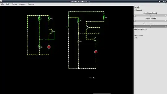
simulate this circuit – Schematic created using CircuitLab


