6

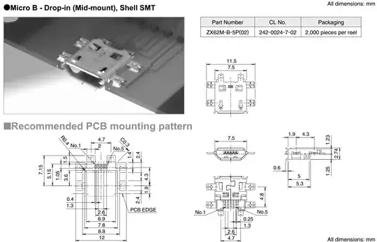
This USB micro B has 6 mounting tabs. If I ground none or only 1 of them, will it ruin the signal? There is a pad for the signal ground that is separate from the mounting tabs.

Fyi USB 2.0 has a max signal rate of 400 Mbps, and an effective payload throughput of up to 35 Mbps, according to Wikipedia.

Is there a general best practice for lazy / layout-confined people to decide how many mounting tabs have to be grounded for a tens-of-megabits connector?

If I only ground one of the tabs, should it be the one closest to the board edge (i.e. to the cable)?

Thanks!

ZX62M-B-5P(02)

AlcubierreDrive
  • 1,484
  • 2
  • 18
  • 26
  • For a high-res version of the image, just right click it and open in new tab. – AlcubierreDrive Sep 11 '12 at 21:51
  • 3
    People are answering a range of questions. *Electrically* grounding one will be enough in almost all cases as unless you have eg multi GHz RF interference the ground will be close enough to ground all over (IMHO as ever). MECHANICALLY connect them all - the more stiffness the better for staying attached to board AND to connector cycle life. HOW you ground may be affected by application. Ground loop can be broken by inductive filtering as per at least one answer. | Copper / vias -> ... – Russell McMahon Sep 11 '12 at 22:29
  • I know ferrite beads will serve at RF, but I don't know about 60Hz and thereabouts. – Scott Seidman Sep 11 '12 at 22:35
  • 2
    http://electronics.stackexchange.com/questions/4515/how-to-connect-usb-connector-shield?rq=1 from our own wiki also shows quite a range of arguments! Seems quite unresolved to me. I can tell you that my own use of commercial usb audio interfaces that cause 60Hz hum and the fairly wide availability of USB isolators pushes me toward the "ground the shield only at the host" school. – Scott Seidman Sep 11 '12 at 22:41

5 Answers5

7

I think normally you don't ground the USB shield on the device side. Instead, you should connect your shield to the chassis/other shielding components, and connect your PCB ground to the USB ground. Between the USB ground and shield you can add a 1Mohm resistor in parallel with a 4.7nF ceramic capacitor.

References:

Cyprus Semiconductor: Common USB Development Mistakes

Atmel: USB Hardware Design Considerations

edit:

did a little more digging, and for higher speed connections it seems like you do tie the shield to ground? I'm not entirely positive about this.

How To connect USB connector shield

plu
  • 671
  • 9
  • 18
helloworld922
  • 16,600
  • 10
  • 54
  • 87
  • 1
    That recommendation to ground both ends of high-speed connections basically says "you'll get noise and ground loops, but because its digital you don't care". Well, if you have something like an A/D on your USB device, you'll care! I think the wide range of practices we're seeing suggests that following rules of thumb by rote will eventually bite, and safest practice is to put real thought into how you treat the shell of the USB connector on each design. – Scott Seidman Sep 12 '12 at 13:01
  • To the best of my knowledge, 1M resistor/4.7nF cap is the right approach. Do not connect the tabs directly to ground, you will create a ground loop. Instead, use a 1M resistor (which will slowly drain any charge that builds up on the shield) in parallel with a 4.7nF cap. The cap makes it so the shield at high AC frequencies appears grounded on both ends (blocking EMI), while at DC it appears grounded only at the host (blocking ground loops). – ajs410 Sep 12 '12 at 17:41
  • 1
    According to Dr. Howard Johnson (http://www.sigcon.com/Pubs/news/2_2.htm), grounding at both ends of the shield should be done for high-speed low-impedance signals. For such signals, "most near-field energy...is in the magnetic field mode", and only a double-grounded shield can effectively block magnetic fields. For low-speed high-impedance signals, most near-field energy is in electric field mode, and a capacatively coupled shield will block most of this energy. – ajs410 Sep 12 '12 at 17:50
  • Finally, I believe it's recommended practice to connect shield tabs/pins to *chassis* ground instead of *signal* ground. This also applies to coupled shields, so in this specific example, you would capacitively couple the shield to chassis ground instead of signal ground. – ajs410 Sep 12 '12 at 17:51
5

The main function of the mounting tabs, besides of course providing ground connection, is to hold the connector in place and prevent it from damaging the tracks on the PCB during connection of the cable.

Bruno Ferreira
  • 4,470
  • 2
  • 25
  • 36
  • Yes, I know.... – AlcubierreDrive Sep 11 '12 at 21:52
  • @Evolved_AI By connecting them to the ground plane you usually have a stronger assembly. – Bruno Ferreira Sep 11 '12 at 21:53
  • To clarify: I fully intend to solder all of them to a pad. I just don't want to add the vias to the ground plane unless there's a reason to do so. And I'm curious about the signal integrity side of this. – AlcubierreDrive Sep 11 '12 at 21:56
  • @Evolved_AI I see no reason why it shouldn't work even if the pad you choose to ground is not the closest one to the signal lines. – Bruno Ferreira Sep 11 '12 at 22:03
  • @BrunoFerreira: But I've read a few references (including those in helloworld922's answer) stating that the mounting tabs (being part of the "USB shield"), should go via a parallel resistor/capacitor on the way to ground, instead of direct connect to ground. – boardbite Sep 12 '12 at 05:17
3

It's not clear to me. http://www.hardwarebook.info/Universal_Serial_Bus_%28USB%29#Shielding says to connect the shield to ground only at the host, which makes sense from a ground loop perspective, but the discussion at http://forum.allaboutcircuits.com/showthread.php?t=58811 shows standards that point to direct connections, connections through a ferrite bead, and connections through a capacitor!

The big cahuna, the USB2.0 Standard at http://www.usb.org/developers/docs/, says

6.8 USB Grounding The shield must be terminated to the connector plug for completed assemblies. The shield and chassis are bonded together. The user selected grounding scheme for USB devices, and cables must be consistent with accepted industry practices and regulatory agency standards for safety and EMI/ESD/RFI.

Scott Seidman
  • 29,274
  • 4
  • 44
  • 109
3

The tabs soldered to the board are an essential part of providing a secure mounting of the connector to the board.

I'm reading comments here regarding your not wanting to put vias by every tab into the GND plane. What in the world are you trying to save here??

BTW, I have actually found that vias actually can play a role in making a pad stay on a board more securely than just a free copper area.

Michael Karas
  • 56,889
  • 3
  • 70
  • 138
  • "What in the world are you trying to save here??" Haha, well said. I'm just curious whether the practice of grounding any/all of those mechanical connections actually serves a purpose or is just a cargo cult. – AlcubierreDrive Sep 11 '12 at 22:18
  • "vias actually can play a role in making a pad stay on a board more securely" You mean via-in-pad? Isn't that considered a dangerous practice b/c it can wick the solder away from the intended joint? – AlcubierreDrive Sep 11 '12 at 22:20
  • Or do you mean keeping the copper trace itself (not the solder) from peeling off the board? Hadn't even thought of that consideration. – AlcubierreDrive Sep 11 '12 at 22:21
  • 1
    @Evolved_AI That was just what I was talking about on my answer. I'm not a native English speaker so I could not find the right words to describe it. – Bruno Ferreira Sep 11 '12 at 22:41
  • 1
    @Evolved_AI - The vias would go to the side of the pads away from the solder area. If you were laying out a board for a hand build type application with soldering iron there would be no problem with putting the via in the solder area. The via in pad for SMT lead only becomes a problem when you are screening on solder paste and doing reflow on the board. That said, I have seen numerous designs that have had vias in solder pads on production SMT boards. In particular these were in the thermal pads under IC packages to help transfer heat from the chip down into the copper planes in the board. – Michael Karas Sep 12 '12 at 07:43
1

Ground all of them; I can't imagine what you would save if you aren't making millions of the boards (literally). You can't run signals there. If they aren't through-hole, just pads you aren't effecting the lower layers.

Brian Carlton
  • 13,252
  • 5
  • 43
  • 64
  • I'm definitely going to solder every tab to a pad. I'm just curious whether the vias from those pads to ground are needed for signal integrity. – AlcubierreDrive Sep 11 '12 at 21:59