0

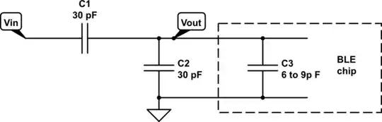
I am using an SiT1552 MEMS TCXO providing 32.768 kHz. It will be sourcing two ICs: a microcontroller and a DA14580 Bluetooth Low Energy transceiver.

The ICs and TCXO are all powered by 3.3V. The TCXO output is the standard 10%-90% LVCMOS voltage swing. It can drive up to 100 pF. It is not AC-coupled.

The MCU is happy with this voltage swing. It wants ~50% duty cycle.

The BLE clock input, however, is internally AC-coupled and needs a 0.1 - 1.5V (pk-pk) voltage swing.

In an app note which requires registration to view, it suggests to use a series capacitor for attenuation:

tcxo_attenuation

I can do this with a larger cap so as to attenuate the signal even more. The TCXO can handle the extra load.
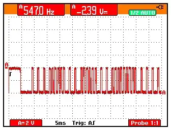
Here is the result.

  • Does it look sane?
  • Will the MCU remain happy?
  • Is there a better method?

.

schematic

simulate this circuit – Schematic created using CircuitLab

bitsmack
  • 16,747
  • 9
  • 52
  • 108

3 Answers3

3

No, you want a smaller value series capacitor (higher impedance) in order to get more attenuation.

For example, if you use a 6.8 pF series capacitor with the load capacitance of 6-9 pF, you'll reduce the signal amplitude to about half its original value.

If you're trying to reduce a 3.3Vpp to less than 1.5Vpp, you'll want an even smaller value. If the load capacitance is just 6 pF (worst case), then the series capacitor should be no larger than 5 pF. Try 4.7 pF (next lower standard value).

Otherwise, looks fine.


Of course, these values are very tiny, to the point where parasitic capacitances could seriously affect the results. To mitigate this, you could add an additional external capacitor in parallel with the input capacitance of the BLE chip:

schematic

simulate this circuit – Schematic created using CircuitLab

Note that this arrangement still limits a 3.3Vpp input to 1.5Vpp going to the BLE chip. The source sees a net capacitance of a little more than 15 pF to ground as its load.

Dave Tweed
  • 168,369
  • 17
  • 228
  • 393
1

It should work. Try a quick simulation if you want some reassurance. Give yourself a bit of margin - don't push the clock amplitude into the BLE module too near the upper limit.

Edit: Dave Tweed is of course right about the coupling capacitor's reactance.

The increased capacitive load on your TCXO output will increase power dissipation a small amount; look at this aspect if this is an ultra low power application.

amb
  • 511
  • 2
  • 5
0

Whilst I respect the fact you have an app note, I would be careful about the use of a capacitive divider to reduce the signal level. I don't believe this is a good plan for two main reasons:

  • The "load" capacitance is so small, that the overall divider will be dominated by stray capacitances
  • The DC bias level of the BLE input is going to be set by relative leakage values of the capacitors in question.

Together this is a recipe for unreliable operation.

In this case you are looking to reduce the ~3V swing to ~1.5V, and move the DC bias point from ~1.5V to ~0.75V. The ratio in both cases is 2:1, so just use a 2:1 resistive divider. Anywhere in the 100K-1M region should give you reliable operation for these kind of clock frequencies.

For higher frequencies, where you just need to move the bias level, a combination of AC coupling and divider rebiasing works well.

This is exactly what I used to couple a 3V3, 0.8V p-p TCXO to the 1.8V crystal input of RPi https://raspberrypi.stackexchange.com/questions/74482/switch-out-the-x1-oscillator-on-a-rpi-2-3

colintd
  • 2,018
  • 2
  • 17