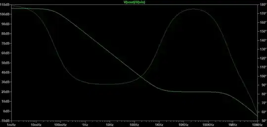
I used the LTpsice to simulate the feedback performance of a integrator circuit with op amp LF356 which is a JFET input op amp but I go strange results (see the image below). The model of the LF356 was the Pspice model downloaded from the TI website (http://www.ti.com/product/LF356/toolssoftware). For this circuit, if I understand correctly, the gain at the low frequency should be as high as the open loop gain of the op amp which is ~100 dB according to the datasheet while at the high frequency (before the secondary pole frequency) should be 20 dB. However, from the simulation results, I only got something like 19 dB gain at low frequency and 15 dB at high frequency. Just to verify that I didn't make any mistake when importing the op amp model, I did the same simulation with another op amp (OPA627) and the simulation results were reasonable (see image below).
  All of this makes me wonder if there is anything wrong with the spice model of LF356 downloaded from the TI website (which seems not likely) or if there is something about this JFET input op amp I didn't understand (not suitable to use for integrator circuit). I would appreciate if anybody could clarify this.
- 43
- 1
- 4
-
Definitely a bad model – Tony Stewart EE75 Jul 05 '18 at 22:12
-
May I ask you for what purpose you have a resistor in the feedback path? An ideal integrator has only a single capacitor as feedback element - and a real one needs (for proper DC biasing) a PARALLEL resistor (as large as possible). – LvW Jul 06 '18 at 08:56
-
Hi @LvW, I was actually trying to simulate the performance of a PI feedback circuit. What I want is the high gain (as much as possible) at low f and a constant gain at relative high f. It may not be proper to call such a circuit as an integrator circuit. – B.J. Jul 06 '18 at 18:55
-
Yes - it is somewhat confusing to ask for integrator information although a PI block is needed. In any case, you need a parallel resistor because of proper DC biasing - unless this block is part of an overall DC loop. – LvW Jul 07 '18 at 09:30
2 Answers
I have seen similar issues in the past with LTspice and from my experience it comes down to the dc operating point.
Let's take a look. This is your circuit:
Look at the dc operating point of the output (~13V) (red box in the picture), essentially saturating and not in the linear region anymore. Even though, your input source has 0 Vdc, you still amplify some dc signal—that is the offset voltage.
For the LF356 this is spec'd at 10mV and this is being amplified by the huge dc gain of the circuit. This messes up the dc operating point and you no longer have meaningful results.
To have meaningful results, you want the dc operating point of both the input and output to be about the same—after all, the bode plot never shows an exact 0 Hz frequency. So if you have 0 Vdc at the input plus the ac signal, you should have 0 Vdc at the output plus the ac signal times whatever gain you have.
I think in the model, they use a value of 3mV for the offset voltage. Go in there and change it to, say, 100uV—you'll see what the effect of the offset voltage is, a real limitation. They call it EOS in the model file. For example, I set EOS= 40uV (which is what the model for the OPA627 uses) and look at the response:
Why did you get good results for the other opamp (OPA627) on the first try? Its offset voltage is listed at 100uV max on the datasheet (they use about 40uV in the LTSpice model) and it does not saturate your output in simulation:
Since the offset voltage is so low compared to the LF356, you see that even though the circuit still amplifies the offset voltage, it doesn't get to the point of saturating the output and you get results as expected in the linear region. The opamp is still providing a gain of 500mV/40uV = 12,500V/V to the dc offset, but since the offset is small, it causes no problem in simulation.
You could ideally resolve the issue by adding a large resistor to the feedback impedance formed by \$R_F\$ and \$C\$. The problem, however, is that you already have a large resistor there (100k), that forces you to pick a value much greater so that at high frequencies the orginal feedback impedance still dominates. Also, the greater the value of this parallel resistor, the greater the dc gain to the offset and risk of saturation. I tried a few values, and the highest I could go was 40Meg (just on the brink of saturation):
It shows improved behavior but still really close to saturation (~11.7Vdc at the output).
Now, this is a method a use sometimes, because it forces the dc operating point to be the same at the input and output (this is similar to find the loop gain for stability analysis). Look at the location of the ac source now:
That arrangement makes both the input and output be at the same dc level and keeps the opamp in the linear region. I am 'injecting' a voltage and measure the gain around the loop. You can look at this answer(towards the end of it) or this video, it explains a bit more why this works.
And this is finally the ac response for this setup:
Hope this helps.
- 5,534
- 1
- 18
- 23
-
I'd really appreciate that whoever downvoted please explain what makes my answer wrong. It does answer the question and adds some value too, of course imho. – Big6 Jul 06 '18 at 15:41
-
Hi @sixcab, thanks a lot for your very detailed reply and it totally clarifies what I confused about LF356. Following your point on the input offset voltage of 3mV of LF356, I added such amount of DC value in my signal source of my original diagram and repeated the simulation. The result now looks right now. My only concern now is, for the practical use of LF356, ~3 mV EOS is always there. If I want to build an integrator circuit like this, does this EOS always saturate the output of the circuit? If so, how to implement the integrator circuit with op amp having mV EOS in practice? – B.J. Jul 06 '18 at 18:50
-
@B.J. You have to make a tradeoff. You'd ideally use a large resistor in parallel with the feedback impedance, that way you can keep the offset voltage from saturating the output. But you want high gain at dc—not good with the offset. So choose an opamp with better offset specs is an option. You could downsize the value of Rf to, say, 20k. Then you can choose a parallel resistor of, for example, 100k, in parallel with the feedback impedance. At dc, the gain would be about 11 and the offset will produce an output of about 33mV. Of course, this changes the characteristics of your circuit. – Big6 Jul 06 '18 at 20:02
The first thing to do is check the datasheet with the model:
Do those plots even look remotely close to you? They don't to me. This is probably a crap model, which is very common.
Upon further inspection the 1db crossover point is ~10kHz in the model whereas the datasheet has it pegged at 11Mhz. What could be the cause of this discrepancy? Maybe the datasheet has the wrong plot, or the wrong schematic for that test, or maybe the model is wrong.
The thing I like to do is look at the spice file for any further clues, the first thing I notice is this:
* 1. Input resistance (Rin) for these JFET op amps is 1TOhm.  Rin is
*    modeled by assuming the option GMIN=1TOhm.  If a different (non-
*    default) GMIN value is needed, users may recalculate as follows:
*    Rin=(R1||GMIN+R2||GMIN), where R1=R2,
*    to maintain a consistent Rin model.
So they mainly were concerned at modeling the amazing 1TΩ input impedance of this amp, but they don't say anything about the gain, GBW or other frequency effects of the stages. I'm willing to bet they left it at that, from what I've seen in the past with other models this is usually the case. You could modify the model yourself and make it better (if its worth your time). Most models are crap and only get 50%-75% of the parameters right. The poles for the second and output stage are probably wrong.
*//////////////////////////////////////////////////////////////////////
* (C) National Semiconductor, Inc.
* Models developed and under copyright by:
* National Semiconductor, Inc.

*/////////////////////////////////////////////////////////////////////
* Legal Notice: This material is intended for free software support.
* The file may be copied, and distributed; however, reselling the
*  material is illegal

*////////////////////////////////////////////////////////////////////
* For ordering or technical information on these models, contact:
* National Semiconductor's Customer Response Center
*                 7:00 A.M.--7:00 P.M.  U.S. Central Time
*                                (800) 272-9959
* For Applications support, contact the Internet address:
*  amps-apps@galaxy.nsc.com
* ///////////////////////////////////////////////////////////////////
* User Notes:
*
* 1. Input resistance (Rin) for these JFET op amps is 1TOhm.  Rin is
*    modeled by assuming the option GMIN=1TOhm.  If a different (non-
*    default) GMIN value is needed, users may recalculate as follows:
*    Rin=(R1||GMIN+R2||GMIN), where R1=R2,
*    to maintain a consistent Rin model.

*//////////////////////////////////////////////////////////
*LF356 Monolithic JFET-Input OP-AMP MACRO-MODEL
*//////////////////////////////////////////////////////////
*
* connections:    non-inverting input
*                 |   inverting input
*                 |   |   positive power supply
*                 |   |   |   negative power supply
*                 |   |   |   |   output
*                 |   |   |   |   |
*                 |   |   |   |   |
.SUBCKT LF356/NS  1   2  99  50  28
*
*Features:
*Low input bias current =             30pA
*Low input offset current =            3pA
*High input impedance =              1Tohm
*Low input offset voltage =            1mV
*
****************INPUT STAGE**************
*
IOS 2 1 3P
*^Input offset current
R1 1 3 1E12
R2 3 2 1E12
I1 99 4 100U
J1 5 2 4 JX
J2 6 7 4 JX
R3 5 50 20K
R4 6 50 20K
*Fp2=20 MHz
C4 5 6 1.9894E-13
*
***********COMMON MODE EFFECT***********
*
I2 99 50 4.65MA
*^Quiescent supply current
EOS 7 1 POLY(1) 16 49 3E-3 1
*Input offset voltage.^
R8 99 49 50K
R9 49 50 50K
*
*********OUTPUT VOLTAGE LIMITING********
V2 99 8 2.63
D1 9 8 DX
D2 10 9 DX
V3 10 50 2.63
*
**************SECOND STAGE**************
*
EH 99 98 99 49 1
F1 9 98 POLY(1) VA3 0 0 0 1.5944E7
G1 98 9 5 6 2E-3
R5 98 9 100MEG
VA3 9 11 0
*Fp1=31.96 HZ
C3 98 11 49.9798P
*
*********COMMON-MODE ZERO STAGE*********
*
G4 98 16 3 49 1E-8
L2 98 17 530.52M
R13 17 16 1K
*
**************OUTPUT STAGE**************
*
F6  99 50 VA7 1
F5  99 23 VA8 1
D5  21 23 DX
VA7 99 21 0
D6  23 99 DX
E1  99 26 99 9 1
VA8 26 27 0
R16 27 28 20
V5  28 25 -.25V
D4  25  9 DX
V4  24 28 -.25V
D3   9 24 DX
*
***************MODELS USED**************
*
.MODEL DX D(IS=1E-15)
.MODEL JX PJF(BETA=1.25E-5 VTO=-2.00 IS=30E-12)
*
.ENDS
*$
- 75,799
- 36
- 80
- 208
