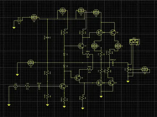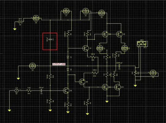
The only DC input to R5 is the R10/R9 voltage divider output. This divide ratio was apparently chosen to result in a particular voltage across R14 when the output rail is at its midpoint. Q5 then acts like a current sink that works against R5 to set the bias point of Q1 and Q6. Those in turn control the high and low side drivers.
The DC voltage of the output rail is therefore set by the R10/R9 divider. You should make sure that this DC output voltage is close to half the supply voltage. If not, adjust either R10 or R9 a little bit to make it so.
The quiescent current of the final output stage is poorly controlled. The final high and low side drivers (Q8,Q9 high side, Q2,Q10 low side) could even be mostly off with no input signal. With signal, they are turned on more, and could dissipate significant power then.
This is a dubious design. Run away. You can find better out there. The way the output stage current is controlled seems to be relying on the fact that it will be low with no signal. That relies on minimum gain of some of the transistors, and will also result in crossover distortion. The complete lack of global negative feedback for the signal is also troubling. Then what the heck is C1 supposed to accomplish?
Run away.


