6

EDIT: After taking all what you guys said into account, I edited the pcb into the following. Changed the FTDI while breaking the ground loops and working on the traces a bit, changed the size of the 100uF capacitor and hopefully the new routing is better.Give me your thoughts over thatenter image description hereenter image description herenearly identical circuit just added the ISP and removed FTDI enter image description here
enter image description here

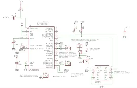
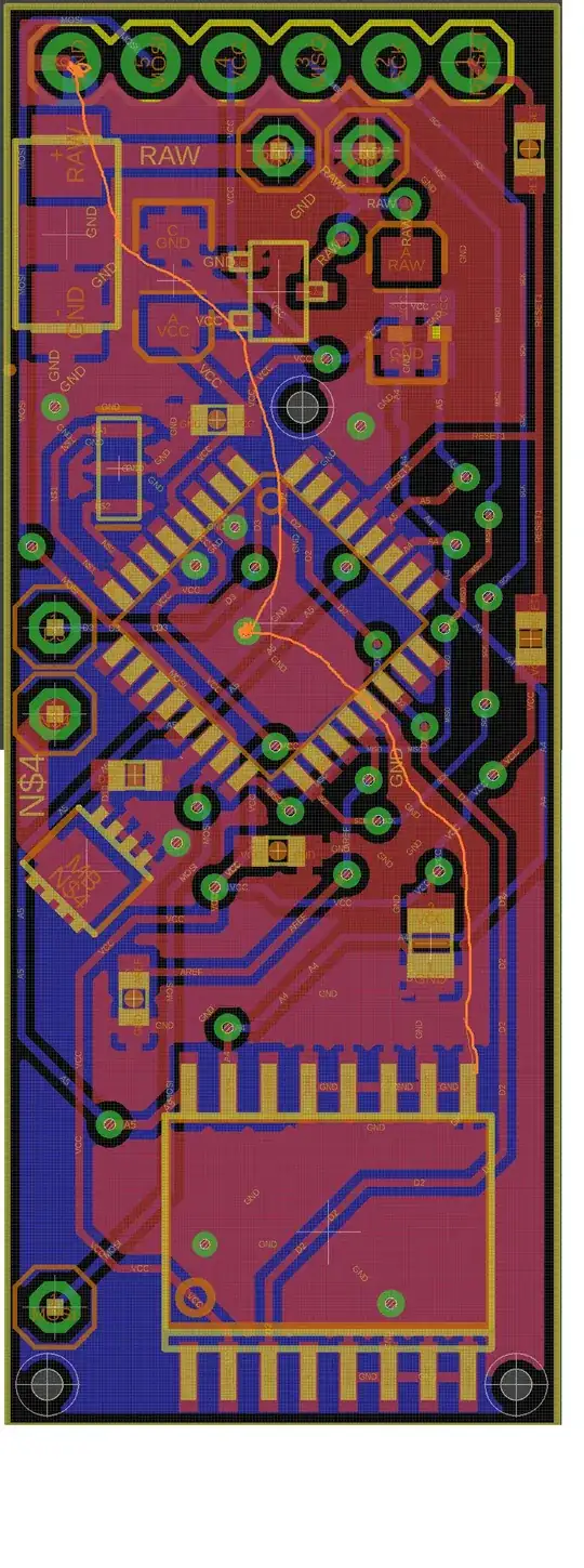
enter image description here So I've drawn an arduino based pcb with the purpose of using a ds3231 temperature compensated RTC to wake up and put to sleep an atmega328p-au which will then control a MOSFET which connect to the ground side of a micro servo to turn it on/off. It's my first design so before I make a prototype I would like to take your opinion about it (attached an online gerber viewer for you guys to take a look Here ). Board size: 45mm*16mm

so the rtc send signals from its digital and analog pins to the arduino, which use that to drive on/Off the MOSFET gate. apart from the motor who have a peak of 1A @5V, everything else is relatively low powered (with a maximum of 40-50mA) . What I'm worried about is interference which might trigger or prevent the trigger of the ds3231 to the MCU. here are more pictures if you don't want to check the gerber:

Sorry for my poor formatting: it's my first time over here. Thank you for your help! The servo (mg90s microservo) is going to be off for like 59min each hour and when it turns on it only do so for a few minutes. I started from the pro mini official drawings and went from there. I used the breadboard prototype I did as a reference for connections. I understand I got a lot to learn. The shipset is in sleep mode almost all the time.

I'm afraid of unwanted noise on the digital pins or A4 A5 which might cause unwanted behaviour(early wake ups).It's powered by batteries. do I risk a lot of noise over the long D2 line Due to the ground plane under the IC1? do A4/A5 have a risk of being affected by noise ? how can I fix that in that case?
  • Are you going to use shield twisted wire pairs for interface? What are specs on motor 5V/DCR? vs FET RdsOn heat rise? Do you care about Gnd noise getting into Agnd? Shielding? Acceptance criteria for all interfaces? – Tony Stewart EE75 Jun 20 '18 at 13:41
  • The NMOS connected to SER is for the motor I guess? What type is the NMOS? I see no flyback diode, the NMOS has a diode in its symbol which might be good enough. To be safe I would add a flyback diode across the NMOS anyway. You can always not mount it if not needed. Just make sure the tracks carrying the motor current are wide. You don't have any sensitive points in your design, most signals are digital so I would not expect interference from the motor to be an issue. – Bimpelrekkie Jun 20 '18 at 13:42
  • 1
    I would take another look at the decoupling of the atmega as far as i can see in the schematic, you have only one cap for the atmega vcc pin while it is common practice to have a capacitor at every Vcc pin located as close to the pin as possible... Furthermore i don't see the I2C lines actually connected to the microcontroller, I see A5 and A4 labels at the RTC ic, but i dont see the same labels placed on the A5 and A4 atmega pins. – Remco Vink Jun 20 '18 at 14:22
  • My feedback is that you have some learning to do regarding drawing decent schematics. What you show here would never pass muster at any engineering design shop. – Michael Karas Jun 20 '18 at 14:47
  • 1
    Somebody needs to read this: https://electronics.stackexchange.com/a/28255/41856 – DerStrom8 Jun 20 '18 at 15:49
  • 1
    The A4 and A5 nets do not connect to the ATmega328's A4 and A5 pins. Net names are not automatically assigned. *Without an offpage flag (like on A0-A3 and A6-A7), U1 pins 27 and 28 only connect to the pullup resistors, they do not connect to the A6/A7 nets.* When the netname is set implicitly (like on IC1 pins 16 and 15), without using offpage flag symbols, it is very easy to miss the connection or lack thereof. (Arduino Pro Mini schematic does have some similar style issues, e.g. the Reset net... I got burned by this some years ago.) – MarkU Jun 20 '18 at 20:48
  • 1
    Your instinct to review this design before fabricating boards is very good, that's a good habit. Back up your schematic (I assume you already keep it in a git repo), review https://electronics.stackexchange.com/a/28255/41856 and spend some time re-arranging things to make the signal flow more obvious. In doing this you'll also be checking that there are no other orphaned nets (like A4 vs U1 pin 27). Also add notes text on the schematic, describing where the mg90s servo motor is connected and where battery power comes in. – MarkU Jun 20 '18 at 20:48
  • 1
    Thanks for your feedback. I will fix the schematics today and update the thread – haidar elie Jun 21 '18 at 03:26
  • You really shouldn't low side switch power to an RC hobby servo to which you are presumably(?) driving a ground-referenced PWM signal. You should use a high side switch. If you insist on doing it the way planned, you should carefully examine what happens during power switching and while power is off. – Chris Stratton Jun 21 '18 at 14:57
  • So you mean i should instead put the mosfet on it's VCC line? Can I ask you why (Curiosity for knowledge at least :) ) ? I tried that same configuration on the breadboard and behaviour was as intended (except noise but adding the capacitor fixed that) – haidar elie Jun 21 '18 at 15:06
  • 1
    You should try tracing out the current loop to the servo, and maybe the micro as well. It's hard to tell whether you have ground traces that you just put a spotty ground pour over, or if your ground path is really as circuitous as it looks. – Drew Jun 21 '18 at 15:14
  • In fact I did those loops intentionally, thinking that it would allow for the shortest path possible for the current to go through... But looking at it again it seems that it might be problematic and might cause current to flow back. thanks for your feedback – haidar elie Jun 21 '18 at 15:21
  • 1
    There's no way to program your MCU! It's possible to use the serial lines for programming after an appropriate bootloader has already been programmed onto the MCU, but the chip is initially empty. You need to bring out the SPI lines (MOSI, MISO, SCK) and RESET for in-circuit programming. –  Jun 21 '18 at 16:40
  • after looking through I can remove FTDI all together and just use ISP with lesser holes and the same connections can be used for bootloader – haidar elie Jun 21 '18 at 19:20

1 Answers1

2

If your worried about noise, make sure you look at return current paths. The ground should be solid and provide a clear pathway to run back to the source (pin 6 on the 0.1" header)

The vias that run between the discontinuous ground planes add 5-10nh of inductance and a few milliohms of resistance. The key is to be aware of it, if your having problems that might be the source. Print the schematic out and draw the vias in as inductors/resistors and see if that poses a problem for the design.

The orange line shows roughly the path the return current from IC1, it doesn't look great as there is only one via on it's return.

Make at least the left hand side of the board a continuous ground.

enter image description here

The ground plane doesn't look great, it may not matter, but if there is a problem it may be hard to track down.

Voltage Spike
  • 75,799
  • 36
  • 80
  • 208