Class-A amplifier design overview
After watching those two videos, Single transistor, 1W and Adventures in a one transistor audio amplifier, I had to illustrate a slightly more sane design approach. To start out, here's the basic idea about how to drive a speaker (without having to find and use a flux-limiting, gapped, audio transformer -- which you will definitely need if you plan to run DC current through the primary):
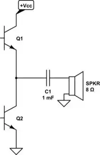
simulate this circuit – Schematic created using CircuitLab
\$Q_1\$ is an emitter follower and it will be able to source current into the speaker. \$Q_2\$ is a common emitter and it will be able to sink current from the load. Together, they can do a fair job of sinking and sourcing current.
A 3rd BJT provides the voltage difference required:
simulate this circuit
Note that I've shown two schematics.
On the left, I've connected the speaker slightly differently (which would also work fine) in order to help segue into the transition on the right. I've also added the 3rd BJT that's needed. On the left is also a current source above \$Q_3\$ and a small resistor to sink a little excess current.
On the right, I've bootstrapped the design to provide the current source indicated on the left. Capacitor \$C_1\$ will develop a voltage across it that remains fairly fixed. Also, \$Q_1\$'s \$V_\text{BE}\$ will have a relatively fixed voltage across it, too. As a consequence, resistor \$R_2\$ will have a nearly fixed voltage across it. So it will form the equivalent of a constant current source. Just what we needed.
Class-A amplifier design details
The design is already taking shape. But it's time to put some parameters into it. In this case, \$V_\text{CC}=12\:\text{V}\$ (in keeping with one of the videos.) I'd like to leave about \$1.5\:\text{V}\$ \$V_\text{CE}\$ headroom for the two BJTs, \$Q_1\$ and \$Q_2\$, to keep them out of saturation and having some decent \$\beta\$ left over. This means that I've got about \$12\:\text{V}-2\cdot 1.5\:\text{V}=9\:\text{V}\$ of remaining swing feeding into \$C_1\$. So \$V_\text{PEAK}=\frac{9\:\text{V}}{2}=4.5\:\text{V}\$, or \$V_\text{RMS}=\frac{V_\text{PEAK}}{\sqrt{2}}\approx 3.2\:\text{V}\$.
The maximum power into the speaker will then be about \$\frac{V_\text{RMS}^2}{8\:\Omega}\approx 1\frac{1}{4}\:\text{W}\$.
We can estimate the peak current to the speaker now as \$\frac{4.5\:\text{V}}{8\:\Omega}\approx 560\:\text{mA}\$. \$Q_2\$ will have to sink that much current, plus some added current to stay in class-A operation. Let's set this minimum to about \$100\:\text{mA}\$. So the peak collector current for \$Q_2\$ (and the peak emitter current for \$Q_1\$) will be about \$660\:\text{mA}\$. Assuming an active \$\beta=60\$ (we can achieve that), this means the peak base currents will be on the order of \$11\:\text{mA}\$.
At this point I'm going to select the D44H11 BJT in the TO-220 package, knowing that I'm going to burn a watt or two in each. From the datasheet I estimate a peak \$V_\text{BE}\approx 800\:\text{mV}\$. I'd like to sink about \$1.5\:\text{mA}\$ with \$R_1\$, so this suggests \$R_1=\frac{800\:\text{mV}}{1.5\:\text{mA}}\approx 533\:\Omega\$. So I'll set \$R_1=560\:\Omega\$.
I will want the needed \$11\:\text{mA}\$, plus this added \$1.5\:\text{mA}\$, in \$R_2\$. So \$R_2=\frac{6\:\text{V}-800\:\text{mV}}{11\:\text{mA}+1.5\:\text{mA}}=416\:\Omega\$. I'll set it a little hotter to \$R_2=390\:\Omega\$.
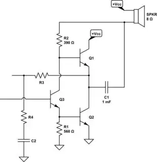
Let's update the schematic:
simulate this circuit
NFB will be required to linearize the output and to set the AC gain. So I've added that feedback network above, with the addition of \$R_3\$, \$R_4\$, and \$C_2\$. I'm going to choose an AC gain of \$15\$, so \$R_3=15\cdot R_4\$.
Since \$Q_3\$ kind of makes up a Darlington with \$Q_2\$, the base current required for \$Q_3\$ will be on the order of \$\frac{13\:\text{mA}}{\beta=150}\approx 90\:\mu\text{A}\$. (It will often be less, but this is safe.) So this means I want a collector current for the fourth BJT to be about 10X more, or about \$1\:\text{mA}\$. \$C_2\$ just needs to be "big enough." I could get into the details to show that \$1\:\mu\text{F}\$ might be fine. But let's make it 10X bigger. So \$C_2=10\:\mu\text{F}\$.
Let's plug in the 4th BJT so that we can discuss the above details in a better light:
simulate this circuit
Now you can see that I've already put in values for the AC gain resistors and \$R_5\$ (newly added here.) I did this by recalling that I mentioned above that the collector current for \$Q_4\$ should be \$1\:\text{mA}\$. If you recall, I figure that the center voltage feeding into \$C_1\$ will be a quiescent \$6\:\text{V}\$. I'd like to drop about half that across the \$V_\text{CE}\$ of \$Q_4\$ and the rest I split evenly between \$R_3\$ and \$R_5\$. So those values are set. And since the gain is 15, the value of \$R_4\$ is also thereby set, too. As shown on the above schematic.
The only remaining problem is biasing \$Q_4\$. You can see in the above schematic that I've added a few parts to achieve that. Since \$Q_4\$'s collector current is about \$1\:\text{mA}\$, the base current will be well under \$10\:\mu\text{A}\$. I decided to choose about \$80\:\mu\text{A}\$ for the biasing current in \$R_6\$ and \$R_7\$, to make it stiff enough. I need a base voltage for \$Q_4\$ of about \$6\:\text{V}-1.5\:\text{V}-70\:\text{mV}=3.8\:\text{V}\$. So \$R_6=R_7=\frac{3.8\:\text{V}}{80\:\mu\text{A}}\approx 47\:\text{k}\Omega\$.
\$C_4\$ gives me an AC ground for a balanced midpoint. The only remaining thing is to compute \$R_8=\frac{12\:\text{V}-3.8\:\text{V}}{80\:\mu\text{A}}-R_6=55.5\:\text{k}\Omega\$. So \$R_8=56\:\text{k}\Omega\$.
Here's the final schematic:
simulate this circuit
That's a class-A amplifier, educational-level not professional.
(Update: I've added a necessary compensation pole capacitor, \$C_5\$, to the above circuit with a nominal value I think will be about right. It was important in order to roll off the high frequencies. So it's included now.)
I promised to add a class-AB. There are some tweaks needed to deal with discrete BJTs that haven't been included, nor discussions about them. So again, this is more of an educational level -- though if you built it I expect you'd still get passable results from it.
simulate this circuit
It includes temperature and device \$\beta\$ and \$V_\text{CE}\$ matching compensation for the diff-amp and mirrors and a few other areas, as well. Adjustments available for the VBE multiplier so that the quiescent current can be set up where you want it and so that the parabolic thermal response can be tweaked, as well.