20

How does the below circuit work?

I know what resistors, capacitors, and transistors do and have played with them on a microcontroller board, but am I trying to understand the logic of the circuit.

Enter image description here

I assume there is a relationship between the 22 ohm and the 470 ohm resistors.

SamGibson
  • 17,231
  • 5
  • 37
  • 58
stack web
  • 217
  • 2
  • 5
  • 2
    The IN757 is a voltage reference for the transistor which regulates the voltage. This circuit is a poor excuse for a voltage regulator, use a 7809. http://www.circuitstoday.com/voltage-regulators – Voltage Spike Jan 26 '18 at 16:55
  • IMHO it's not sensible to add a new circuit to the question after 4 days, as you've just done. The result would be a mix of answers, some referring to one circuit, some referring to the other circuit and so potential confusion for readers. That is why the rule here is to ask *one* question, so that the answers clearly refer to that question. I recommend you revert back to the previous version of the question (use the rollback feature) and, if you still need help, ask about the new circuit in a new question (link to this one, if relevant). – SamGibson Jan 29 '18 at 18:08
  • In any case I think that my answer below and others give you enough information to understand exactly how that second (first) circuit works. If you post it as another question then please link to this one and explain exactly what you don't understand given all the explanation below. – Transistor Jan 29 '18 at 18:36
  • 1
    I have removed the extra circuit for clarity. THanks all again. – stack web Jan 30 '18 at 23:22

3 Answers3

62

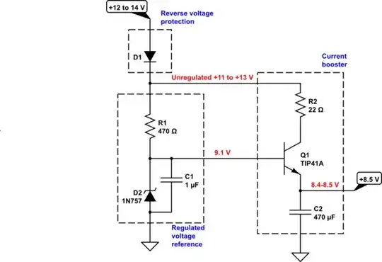
It breaks up into three simple sections that are each relatively easy to explain:

schematic

simulate this circuit – Schematic created using CircuitLab

The first part is the diode that provides reverse voltage protection. If for some reason the polarity of the input voltage is wired opposite to what it is supposed to be, then \$D_1\$ will block it and the output will also be essentially off. Only if the polarity is correct, with the rest of the circuit be operational. The price of including this added protection is a voltage drop of perhaps \$700\:\text{mV}\$. (I exaggerated this voltage drop a little in the diagram. But it gets the point across.)

The next section is below that. It's a zener regulator. The resistor is there to limit the current. The zener tends to have the same voltage across it, when reverse-biased with sufficient voltage (and \$11-13\:\text{V}\$ is more than sufficient.) With \$R_1\$ as given, you'd expect the current to be somewhere from about \$5\:\text{mA}\$ to \$10\:\text{mA}\$. This is a "normal" operating current for many zeners. (You could go look up the datasheet and find out, exactly. I didn't bother here.) So the voltage at the top of the zener should be close to \$9.1\:\text{V}\$. The exact current through the zener will have a slight impact on this. But not much. (The capacitor, \$C_1\$, is there to "average out" or "smooth out" the zener noise. It's not critical. But it is helpful.)

The final section on the right is there to "boost up" the current compliance. Since the zener only has a few milliamps to work with, if you didn't include this added section your load could only draw a very small few milliamps, at most, without messing up the zener's regulated voltage. So to get more than that, you need a current boosting section. This is composed of what is often called an "emitter follower" BJT. This BJT's emitter will "follow" the voltage at the base. Since the base is at \$9.1\:\text{V}\$, and since the base-emitter voltage drop will be about \$600-700\:\text{mV}\$, you can expect the emitter to "follow," but here with a slightly lower voltage (as indicated in the schematic.) This BJT doesn't require much base current in order to allow a lot of collector current. So the BJT here may "draw" current from its collector, by also drawing a much smaller, tiny base current ("stolen" from the zener, so it can't be allowed to be very much), and then this sum of the two becomes the total emitter current. This emitter current can be as much as several hundred times the base current. So here, the BJT might draw \$1\:\text{mA}\$ of base current (which is okay, because there is several times that much available due to \$R_1\$) in order to handle perhaps as much as \$200\:\text{mA}\$ of emitter current. In keeping with the idea of "being conservative" the specification only says \$100\:\text{mA}\$ -- and that's very much the right way to go when telling someone what this is capable of. Be conservative.

\$R_2\$ is there as a bit of a short-circuit current limit. It doesn't serve much else. But if the load tries to pull too much current via the emitter then there will be an increasingly larger voltage drop across \$R_2\$ and this will cause the collector to have access to lower remaining voltage. At some point, the emitter will be "cramped." In this case, a drop of more than \$2\:\text{V}\$ (perhaps a little more) will probably begin the process of cramping the output. This means the limit is somewhere above \$\frac{2\:\text{V}}{22\:\Omega}\approx 100\:\text{mA}\$. Overall, \$R_2\$ is a very cheap way to add some modest protection to help make the whole thing just a little more bullet-proof, so to speak.

Note: \$C_2\$ is an output capacitor providing some added current compliance if there's a momentary, short-term demand by the load. I'd also normally want to include an output resistor across \$C_2\$ (not shown) of perhaps \$4.7\:\text{k}\Omega\$ as a bleed resistor to provide a DC path to ground from the output and to discharge \$C_2\$ after a few seconds, when the input source of power is removed.

jonk
  • 77,059
  • 6
  • 73
  • 185
  • Thanks for this, very clear and helping me get a grasp on transistors. – Russell Borogove Jan 26 '18 at 05:05
  • Thanks, Awesome explanation and I give thanks to all (except 1) who contributed to the question. – stack web Jan 26 '18 at 05:16
  • Great clear answer. – Blair Fonville Jan 26 '18 at 05:49
  • So let me get this. so I assume the R1 , IN757, C1 act like a R1 resister plus a IN757 C1 combination to drop the 11v to 9.1, So the formula R1/(R1+(IN757 C1) cause a 2v drop after R1. So are you saying the IN757 + C1 have resistance to cause the about 2v drop. – stack web Jan 26 '18 at 05:55
  • @stackweb A 1N4007 diode would not allow any current if it replaced the zener, so R1 would have no current and therefore wouldn't drop any voltage. So the entire 11-13 V would be at the base of the BJT in that case. But the zener diode "breaks down" a bit when a reverse voltage in impressed across it -- down to about 9.1 V. So the remaining voltage (diff between 11-13 V and 9.1V) generates a current through R1. This current then flows through the zener to ground. (Except for the base current needed by the BJT.) I hope that makes sense. – jonk Jan 26 '18 at 08:24
  • +1 for great description. I'd add R2 does load share with Q1 allowing the use of a smaller transistor and heat-sink requirements. – Trevor_G Jan 26 '18 at 08:42
  • 2
    @stackweb yes. a zener diode, well any diode really, can be thought of as a device that changes it's resistance to maintain the voltage across itself within some bounds. – Trevor_G Jan 26 '18 at 08:46
  • 1
    @Trevor_G True. There is some dissipation sharing there with R2. I had considered the idea of discussing dissipation but decided that it was beyond the scope of an appropriate answer. I worried that it might even blunt or damage the main points. So I dropped the idea. – jonk Jan 26 '18 at 08:48
  • Yup, that is always a balancing act. The other thing you did not mention is when the current exceeds the drop tolerance on R2 the load pulls much more base current which will pull down the zener. But again, that may be "A Bridge Too far!" :D – Trevor_G Jan 26 '18 at 08:51
  • 1
    @Trevor_G Yeah. I chose the word "cramps" as being sufficient here. The exact details aren't too difficult. But this is a good beginner's circuit to understand and the nuances that the resistor forces saturation and that saturation entails rapid increase in base current which then may remove much or all of the zener's current starts to get to be "too much detail," and therefore again confusing. So I returned to "cramps" as good enough for now. – jonk Jan 26 '18 at 08:54
  • 1
    :) good man. Personally I prefer the word "chokes". I think it's a much better visual, but that may be something Freudian, or Sadistic.. about me LOL – Trevor_G Jan 26 '18 at 08:58
  • 3
    @Trevor_G There aren't enough really good "beginner's circuits," to be honest. This one sits in a really cool "sweet spot" which provides: (1) a useful circuit; (2) can be fabricated and tested on a breadboard; (3) can be checked out with a basic meter almost anyone can get cheaply using common skills; (4) includes enough protection ideas to make it relatively safe to use *and* abuse; and (5) is right at the point where it might be a small struggle to understand and yet still accessible to those with a few basic ideas. – jonk Jan 26 '18 at 09:02
  • Yup it sure is. – Trevor_G Jan 26 '18 at 09:04
  • What does C2 do? Additional zener noise filtering? – Todd Wilcox Jan 27 '18 at 06:14
  • 1
    @ToddWilcox Since this is a voltage regulator, it is assumed that there will also be a load (not shown) between the 8.4 V output and ground. Placing a capacitor there stores some charge and will help reduce variations of the output voltage due to rapid changes in the load requirements. – jonk Jan 27 '18 at 07:57
  • As far as I know, TIP41 is a complementary (Darlington) transistor with two base-emitter junctions in series. So its "base-emitter" voltage should be two times higher... and the output voltage should be no more than 7.9 V. – Circuit fantasist Nov 26 '19 at 23:38
  • 1
    @Circuitfantasist This was a long time ago, but I appreciate the catch very much! Yeah. I just looked at the TIP41 datasheet that I'd looked at "back then." And it didn't mention Darlington but I should have read the VBE spec. Seems like it is. Anyway, when I get a moment of time (not now), I'll review your comment in the context of my answer and update it as appropriate. Thanks! – jonk Nov 26 '19 at 23:49
18
  • The TIP41A is configured as a voltage follower. The emitter voltage will be equal to the base voltage minus about 0.7 V.
  • The 470 Ω resistor provides the base current to turn on the transistor and pull the base towards the supply voltage.
  • The zener diode will turn on if the base voltage goes above 9.1 V (its breakdown voltage). Therefore the base will be held at 9.1 V.
  • There will be about 3 V dropped across the 470 Ω resistor so the current will be \$ \frac {3}{470} = 6 \ \mathrm {mA} \$ approx.
  • The load current will pass through the 22 Ω resistor and the transistor. At 100 mA the resistor voltage drop will be \$ IR = 0.1 \cdot 22 = 2.2\ \mathrm V \$ and the power dissipated will be \$ I^2R = 0.1^2 \cdot 22 = 0.22 \ \mathrm W \$.
  • Dropping most of the voltage across the resistor reduces the power dissipated in the transistor. We'll come back to that.
  • The 1N4007 is to protect the circuit from reverse voltage input connection. We will lose about 0.7 V across it.

Back to the transistor: lets work it out for the maximum 14 V input.

  • Vin = 14 V.
  • V after the 1N4007 = 13.3 V.
  • V after the 22 Ω resistor at 100 mA = 13.3 - 2.2 = 11.1 V.
  • V across the transistor = 11.1 - 8.5 = 2.6 V (allowing about 0.6 V voltage drop between the base and the emitter).
  • Power dissipated in the transistor \$ = VI = 2.6 \cdot 0.1 = 0.26\ \mathrm W \$.
  • Without the 22 Ω resistor the power dissipated in the transistor would be \$ (2.2 + 2.6)0.1 = 0.46\ \mathrm W \$.

I assume there is a relationship between the 22ohms and the 470 ohms.

Not really. They are serving independent functions and don't interact.

Transistor
  • 168,990
  • 12
  • 186
  • 385
2

The key element of this circuit causing it outputting +9 V is zener diode 1N757. When the circuit is supplied with the power (+12 to +14 V) the 1 µF capacitor is discharged, and the transistor is switched off. With some delay, the 1 µF capacitor gets charged through the 470 ohm resistor to the zener diode's nominal voltage, and it opens the transistor up to its emitter having a 9 V output voltage.

The 22 ohm resistor here is limiting the current if something goes wrong (will protect from shortage/overcurrent for short time, but for longer periods transistor may overheat and fry). The 1N4007 diode, as I understand, is to ensure that if you accidentally connect AC input voltage, circuit would not fry from negative the voltage.

Peter Mortensen
  • 1,676
  • 3
  • 17
  • 23
Anonymous
  • 6,908
  • 1
  • 14
  • 41