Having quite good knowledge on what's going on with voltage on transistors won't help you if you do not know how transistor really works. You expect all transistors to work as a switch, but they won't if you leave circuit like that.
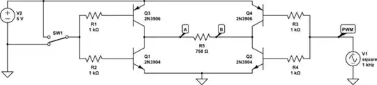
simulate this circuit – Schematic created using CircuitLab
You have following errors:
Transistor Q5 will work as emitter follower (it will not go into saturation as in switch mode). When PWM source on it's base goes to the high state(5v) it may be represented as voltage source with (5 - 0.7) V and internal resistance equal to R5. So voltage on the collectors of the Q1 and Q3 transistors will be something around 4.3 volts. Q1 and Q3 are emitter followers again. But the voltage on it's collector is already 4.3v (and mind the voltage drop on the R5) and emitter-to-ground circuit contains your load resistance (I've met electomechanical ammeters with internal resistance 750 to 4k Ohms) so Q1 and Q3 will not go into saturation when you expect. It may be not so critical if you use it with measuring instrument which have relatively low current consumption, maybe it even will work SOMEHOW (I am not sure) with BJTs in linear modes. But if you want to drive heavy load this circuit is only good for burning transistors. Instead you better try this:
simulate this circuit
Connecting one GPIO pin instead SW1 you can control polarity of the voltage and put the PWM output to other half-bridge. In this configuration all transistors work as a switches. However be aware of shot-through which may happen if there is no voltage source attached instead PWM or SW1. In that case current can flow through Q3 collector-> Q3 base->R1->R2->Q1 base->Q1 collector same applies to other half-bridge(Q3 R3 R4 Q4). This can open lower and upper transistors simultaneously which will result in a short between ground and positive supply. You can avoid this by setting corresponding bits in DDR and PORT registers just after initialization. Other way is to use 4 ATMega pins instead of 2, thus avoiding this situation. You can use 2 regular GPIO pins to control direction (Q3 and Q1) and 2 PWM pins, that resides on the same timer (they are called in following manner: OC1A and OC1B for Timer1), which will generate inverted PWM signals.