I just quickly drew this up, the last hour or so. I agree that with wires on a protoboard such as what you are using, it's important to have lots of bypass capacitance right on the protoboard itself. Include that. However, I think you may also have had problems due to the fact that there is lots of capacitance (a few pF) between each nearby hole on the protoboard, too. And you didn't add some capacitance on the feedback resistor (which may be needed.) The values here are designed around the idea that you can deliver perhaps as much as \$2\:\text{A}\$ peak into an \$8\:\Omega\$ load, so I tried to take that into account. That said, I've really not done anything here but just "pop this out," quickly and roughly. No time for more than that.
simulate this circuit – Schematic created using CircuitLab
Here I set up the Sziklai output driver arrangement with the added \$V_{BE}\$ multiplier present as it should be. I've used two variable resistors, one keeping your \$2\:\text{k}\Omega\$ value (which I guess you have) and another being \$100\:\Omega\$. \$P_1\$ lets you adjust the quiescent current (which you can measure by checking the voltage between the collectors of \$Q_{12}\$ and \$Q_{13}\$.) \$P_2\$ lets you adjust things for temperature and Early Effect compensation. But feel free to completely remove \$P_2\$ and \$R_3\$ by shorting them out, if you want to. They are NOT critical. Just an offering. If you do ignore (short) them, then you may need to pick a different value for \$R_2\$ (smaller, perhaps.) You'll know if that's needed when you find you can't adjust the quiescent current to the right range with \$P_1\$. If so, pick a nearby value for \$R_2\$ and try adjusting \$P_1\$ again.
Feel free to ask questions, Keno. I'll try and answer them as I'm able to. To others, feel free to criticize and kibbitz.
Shoot for a quiescent current (no input signal) of perhaps one milliamp, or so. Adjust \$P_1\$ for that and read it off as I mentioned above. You can work out the voltage you'd need to read. (Feel free to increase the values of \$R_{E_3}\$ and/or \$R_{E_4}\$ to make it easier to pick this out -- just don't drop more than few tenths of a volt while adjusting things there.)
Assuming you need lots of current gain (and you do) for the output driver section, the Sziklai arrangement has a few advantages over the Darlington arrangement:
- There are just two \$V_{BE}\$ drops to deal with.
- These two \$V_{BE}\$ drops are subject to far less heating, so their \$V_{BE}\$ drops are more stable making it easier to plan the \$V_{BE}\$ multiplier behavior.
In the Darlington case, while it is still true that two of the four BJTs have less heating taking place, the fact is that it includes all four \$V_{BE}\$ drops in what is required to be controlled via the \$V_{BE}\$ multiplier. So this compounds the design of the multiplier or else decreases thermal stability. Either way, it's not a good thing in favor of Darlington. So one usually doesn't use it for cases like this.
(In short, I don't know of a good reason to use Darlington, other than part availability issues perhaps. So, for example, if high current PNPs are horrible and/or unavailable, you might replace \$Q_{10}+Q_{12}\$ with a Darlington alternative using only NPN. But you'd still probably keep the Sziklai on the bottom quadrant of the driver.)
Let's look at the current source stripped of some of the "extras." (They aren't important to understand the basic DC operation.)
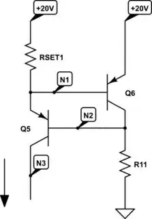
simulate this circuit
Ignoring whatever load there might be for the \$Q_5\$ collector, you should be able to very roughly sketch out in your mind that this circuit will actually bias itself in some fashion. From \$+20\:\text{V}\$, there is a DC path through \$RSET_1\$, the emitter of \$Q_5\$ to its base, then through \$R_{11}\$, which is tied to ground. So there is no question that there will be some active current through that path. If \$Q_6\$ were pulled from the circuit, and assuming that \$Q_5\$ had a collector load to ground (or \$-20\:\text{V}\$) which didn't otherwise cause \$Q_5\$ to saturate, then we could compute the base current as:
$$I_B=\frac{20\:\text{V}-V_{BE}}{R_{11}+\left(\beta+1\right)\cdot RSET_1}$$
And this would be little different from the standard CE amplifier computation.
But in this case there is an added \$Q_6\$. What does it do? Before it is added, there is no particular limit to the voltage drop across \$RSET_1\$. It could be several volts, or more. But with \$Q_6\$ added, which is sensitive to its base-emitter voltage, any voltage drop across \$RSET_1\$ that is larger than about one \$V_{BE}\$ will cause \$Q_6\$ to source lots more current through its collector, all of which must be driven to ground via \$R_{11}\$. This added current causes an increased voltage drop across \$R_{11}\$. (Keep in mind that by adding only a mere \$60\:\text{mV}\$ to the voltage drop across \$RSET_1\$, the collector of \$Q_6\$ will source ten times as much collector current into \$R_{11}\$ which will mean also 10 times the voltage drop across \$R_{11}\$!) This increased voltage drop across \$R_{11}\$ also means that the base of \$Q_5\$ is pushed upwards (towards the positive rail) and this causes \$Q_5\$'s \$V_{BE}\$ to get "pinched", thus reducing its collector current.
What exactly is \$Q_5\$'s collector current? Well, it pretty much is the current in \$RSET_1\$. That's about it. And since we are also pretty certain about the voltage across it (one \$V_{BE}\$), we can compute the collector current in \$Q_5\$ pretty reliably. \$Q_6\$ will be constantly and carefully monitoring its own \$V_{BE}\$ and responding immediately to any changes by adjusting things at \$Q_5\$'s base and "pushing on/sinking current into" \$R_{11}\$ to make those changes work in the right direction.
In the end, there are about two \$V_{BE}\$ drops from your positive rail down to the base of \$Q_5\$. It's collector can "reach" about that high towards the positive rail before it starts saturating (causing other problems.) And this gives quite a lot of compliance range for the collector of \$Q_5\$. Which is a good thing.
In this short-hand version of the circuit found at the beginning of my answer, I removed \$RB_1\$. It's not strictly required for explaining the circuit. But it is added to help with possible oscillation when the circuit is part of a larger system and there is an AC signal being amplified. It doesn't drop much voltage, so you can "mostly ignore it." In general, a resistor of a few hundred Ohms to perhaps a thousand Ohms does the job, but the better value to use does depend on the base current (of course.) It's just not particularly critical-valued.