-3

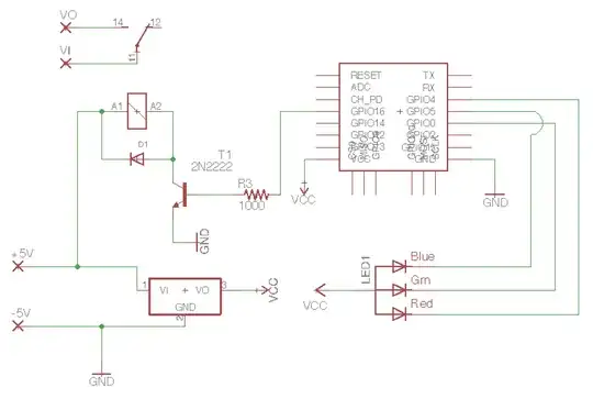
I am trying to make a WiFi controlled relay. I believe that my circuit works fine, but I would like others to look over it before I get it fabricated. The voltage powering the entire system is coming from a 5v AC to DC converter. Here is what the circuit looks like:

Here is my parts list since some of them are unlabeled:

  • Relay: Songle SRD-05V
  • Diode: 1N4148
  • Transistor: 2n2222
  • LED: Microtivity IL612 (Common Anode)
  • WiFi: ESP-12E
Jeebus
  • 91
  • 5
  • Leaving floating inputs is unwise and no Vcc decoupling shown. Relay contact current or voltage transients for EMI is unknown. No POR? – Tony Stewart EE75 Dec 01 '17 at 05:23
  • At the upper left there's a switch for \$VO\$ and \$VI\$, the same labels are used at the bottom left (in the box), which looks like an LDO. Is that a switch for bypassing the LDO? – Harry Svensson Dec 01 '17 at 05:32
  • No current limiting on led and voltage is not high enough for good control of current. R3 too high value. What Tony said, also the esp needs some resistors pull-up/down and the regulator (whatever it is) should have largish caps in the input and output, according to the data sheet. I realize you may not have the rep to include a bunch of links but if possible it is always good to include links to the manufacturers' datasheets for all relevant components. – Spehro Pefhany Dec 01 '17 at 05:35
  • @HarrySvensson That is the default labels for the voltage regulator, they do not have any connection to the AC VO/VI pads. – Jeebus Dec 01 '17 at 05:35
  • @HarrySvensson that's the relay contacts, the vr designators are not net labels so there is no conflict. – Spehro Pefhany Dec 01 '17 at 05:37
  • Sorry I am not familiar with some terminology- what do you mean by POR and EMI? @TonyStewart.EEsince'75 – Jeebus Dec 01 '17 at 05:41
  • 3
    Please read this community wiki answer. You'll find it helps you make better schematics and helps us interpret your schematic easier for your next question. https://electronics.stackexchange.com/questions/28251/rules-and-guidelines-for-drawing-good-schematics – Dan Laks Dec 01 '17 at 06:38
  • EMI=electromagnetic interference. POR = power-on reset. EMI is shorthand for the various compliance tests a product might have to go through to insure it does not cause interference with radio equipment. Power-on reset is almost a thing of the past because most microcontrollers now incorporate it internally. But in the bad old days, you might use an external reset chip to hold the processor reset asserted until the power voltage was above some certain threshold for some certain time. – user57037 Dec 01 '17 at 07:32
  • Except that of mentioned decoupling capacitor, too big R3 and missing limit resistors for RGB diode (is ESP-12E able to provide enough current to lit your LEDs?) you would miss 'Reset' and 'Boot' switches - they can be helpful when you decide to do firmware update later. – smajli Dec 01 '17 at 08:19
  • 2
    I suspect it isn't useful to fill this Q&A website with large numbers of questions titled "check my circuit for me". – RedGrittyBrick Dec 01 '17 at 09:01
  • 3
    You should breadboard this before having it manufactured on a PCB. – DerStrom8 Dec 01 '17 at 12:26
  • 2
    *"... since some of them are unlabeled"* So label them. Duh! – Olin Lathrop Dec 01 '17 at 12:30
  • 3
    This is the third question from you and this is becoming a "slap some parts down at random and get someone to tell me what's wrong with it" design service. The information you need is readily available on-line, either in the part data sheets, or as example schematics. You really need to do your due diligence. The volunteers and specialists here do not have the time to walk you through every step of your design. I see at least seven things wrong with this design. – Trevor_G Dec 01 '17 at 12:59
  • You have to read the datasheets of the components carefully and you should follow their proposed schematics, because in your schematics there are errors and missing components (decoupling capacitors, resistors). – Ange Mechanic Dec 01 '17 at 11:21

1 Answers1

5

You ask about the circuit, but your schematic is too much of a mess to get into that.

Engineering requires attention to detail. For good results, this must be carried out thru the whole design process. A messy schematic is either the product of messy thought, or a Eh, it doesn't matter attitude. Either results in a bad design.

Problems with the schematic include:

  1. No component designators on some parts. This looks like it was done in Eagle. Eagle makes it very easy to show component designators per part. There is no excuse for this.

  2. The labels for the pins sticking out the bottom of the large block collide with the labels of the pins sticking out the side. Surely you could see this for yourself.

  3. The GND symbol below T1 is sideways. You clearly had room to make it right side up. In fact, that would have been simpler. This makes it more effort to look at your schematic, and is just rude.

  4. The flow around T1 is right to left, although it's not a feedback path. It is nice to keep logical flow left to right when possible, and it certainly could have been here with a little re-arranging of parts.

There are some glaring problems with the circuit too, but once you take some care with the schematic, you may find them yourself.
clabacchio
  • 13,481
  • 4
  • 40
  • 80
Olin Lathrop
  • 310,974
  • 36
  • 428
  • 915
  • 2
    @clabacchio: That edit was too heavy-handed. It is important for the OP to realize he is disrespecting and insulting us by dumping slop here. You have removed a important part of the message. – Olin Lathrop Dec 01 '17 at 13:41
  • 1
    I understand, but it is already a borderline answer by itself, since it only touches the actual question. It got flagged for rudeness and that's the least I thought I could do. – clabacchio Dec 01 '17 at 13:59
  • 1
    I'll give a +1 for the original answer. – Harry Svensson Dec 01 '17 at 14:41
  • 1
    I appreciate criticism, but I don’t appreciate the arrogance. I am extremely novice to electronics and judging by my profile I don’t regularly post here. Someone above mentioned I should read over how to make better, more readable schematics, so I will be sure to read over that before posting again. I have no problem taking criticism but when you make it, why assume that the only reasons someone makes mistakes is for carelessness or bad attitude? – Jeebus Dec 01 '17 at 15:27
  • 1
    @Jee: It doesn't require electronics knowledge to know that sloppiness is bad, and asking volunteers to look at your sloppy work is rude. Maybe you didn't know about some of the finer points, but surely you could see for yourself the colliding and therefore unreadable pin names in the large block. The fact that you didn't fix it shows a *eh, who cares* attitude, no matter how much you protest otherwise. It's OK not to know how to draw schematics, but then that's what you should be asking about until you can draw them properly. – Olin Lathrop Dec 01 '17 at 16:07
  • @OlinLathrop Thank you, I will make sure to provide a more orderly schematic next time. – Jeebus Dec 01 '17 at 16:41
  • 1
    @clabacchio Closing this problematic question is more fair than censoring Olin. – Nick Alexeev Dec 01 '17 at 20:00