19

Here's a scan of a "chip-and-pin" Visa Electron contact pad

enter image description here

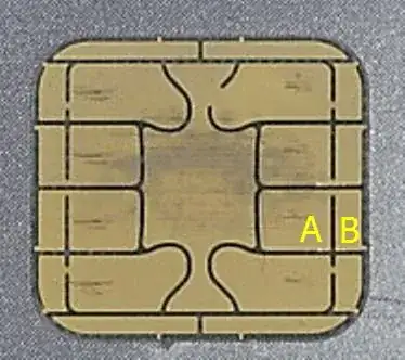
It looks like a metal plate divided into regions by narrow cuts. Look for example at regions marked A and B - there's a cut between them but it only separates them partially and there's a narrow metal bridge left on the top of the cut.

That looks strange. If the regions have to be connected why not just omit the cut entirely and have one single region?

Maybe it's for cleaning contacts of the reader - as they pass over the cuts the dirt if any gets scrapped of them, but I'm not sure.

What's the reason for this design? Why are the regions partially separated by a cut yet there's a conductive bridge left between them?

sharptooth
  • 12,374
  • 26
  • 83
  • 144

2 Answers2

3

The ISO/IEC 7816 (see part 2) standard does not define the shapes of the pads, only the minimum size:

This part of ISO 7816 does not define the maximum dimensions or shape of the contacts except for the requirement that each contact shall be electrically isolated from the other contacts.

Therefore, it is safe to assume that what you see is done just to make it look nice. You can see the same thing with the USB contacts below:

enter image description here

Armandas
  • 7,845
  • 1
  • 32
  • 56
1

While I don't know about those connectors in particular, some similar connectors such as the SmartMedia connector have "odd" shapes for the purpose of improving mechanical robustness. An overly-long straight line without any metal across it can represent a mechanical weak point. Curves can be used to break up such lines. I'll admit it's curious that the sample shown has two straight lines that cut all the way from left to right.

Additionally, a pattern like the one indicated may provide a means of automated electrical testing if a row of four probes touch the card in such a way that two should be on either side of a "mostly-cut" line. If a voltage-limited current voltage is driven between the inner probes, the inner probes should have a voltage across them proportional to the resistance. Also, a company that wanted to indicate the location of each circuit on a panel could do so by slightly altering the positions of those thin interconnects. Such a feature would not confuse people as might a visible number, but could nonetheless be used for troubleshooting manufacturing problems.

supercat
  • 45,939
  • 2
  • 84
  • 143