0

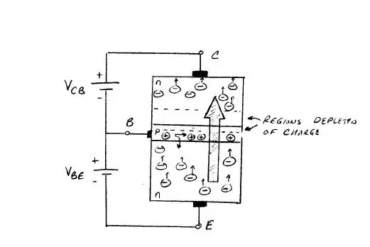
Bjt in active region, physical representation:

enter image description here

In circuit:

enter image description here

Why is that in circuit base connects to emitter? Shouldn't it connect to "P" area, and then collector node and emitter node connect to "P". So P should be in the middle between C and E.

No?

Where is \$ V_{CB} \$ ?

Jack
  • 257
  • 4
  • 12
  • 3
    There are plenty of sites explaining how transistors work. Read the [Wikipedia article](https://en.wikipedia.org/wiki/Bipolar_junction_transistor) for starters. – Finbarr Nov 13 '17 at 17:40
  • Try reading through these two answers from me. See Figure 3.4 shown in [Terminology for BJT 'regions of operation'](https://electronics.stackexchange.com/questions/254391/terminology-for-bjt-regions-of-operation/254397#254397) and then see also [Why is Vbc absent from bjt equations?](https://electronics.stackexchange.com/questions/252197/why-is-vbc-absent-from-bjt-equations/252199#252199). These may help a little. – jonk Nov 13 '17 at 19:14

1 Answers1

1

Break the figure into parts and try to understand.

First consider Base and Emitter ; Base is P and Emitter is N type. Hence they form a diode. Seeing the voltage you can say that they are forward bias therefore there is a current flow from Base to Emitter. (Electrons flow in the opp. direction)

Now consider Base and Collector ; Base is P and Collector is N type. Hence they form a diode as well. Seeing the voltage you can say that they are REVERSE bias therefore there is a NEGLIGIBLE current flow between Base to Collector or other way round. That is why no connection between the two. But there is an interesting thing going on here; since they are reverse biased there is a strong Electric field experienced at the junction of base-collector hence the electrons from emitter entering sees that field and is immediately sucked by that field and hence those electrons reach collector this is the current flow between emitter and collector. This is how BJT work basically, there are many perspectives of the working, follow what suits you the best.
enter image description here

enter image description here

rsg1710
  • 306
  • 1
  • 8
  • well yeah those electrons, if we talk physically, go from emitter to collector then to base then back to emitter again, no?? Yet base doesn't seem to connect to C separately. – Jack Nov 13 '17 at 21:35
  • I think you answering your own question, the electrons flow from emitter to collector or base , where are any charge flowing from base to collector/ collector to base? – rsg1710 Nov 14 '17 at 09:05
  • No, I mean, electrons kinda flow in a loop? They can't just physically go from emitter to collector and "stay" there, then they will go to base - > emitter and back to collector again... No? – Jack Nov 15 '17 at 05:02
  • Not really To be very precise, the electrons flow from emitter to collector (and then to supply) only; but in between in base some of the electrons recombine with the holes in p-type base this leads to base current. – rsg1710 Nov 15 '17 at 09:41
  • Please see the edited answer to understand pictorially. and May be you can ask your queries from this figure. – rsg1710 Nov 15 '17 at 09:43
  • the picture is taken from wikipedia. – rsg1710 Nov 15 '17 at 09:58
  • It is actually enlarged picture of your own figure (first part) – rsg1710 Nov 15 '17 at 10:06
  • >"(and then to supply) only" What is supply here? \$ V_{CB} \$ ? Are you sure electrons in collector don't escape collector area and go in the loop through \$ V_{BE} \$ then \$ V_{CB} \$?? So do the electrons just stay in collector then? – Jack Nov 16 '17 at 02:42
  • Ah haan I think I see the confusion; may be this interpretation will help you; break all the potential differences to voltages i.e. think them as individual sources i.e \$V_E\$,\$V_B\$ and \$V_C\$ the potential difference then still holds good yeah i.e. \$V_{BE}=V_B-V_E\$ and so on. So now you would see a loop for electrons GND to EMITTER to COLLECTOR to GND. I again repeat since the diode between base and collector is reverse biased the current flowing from base to collector is negligible. To help you I have added another fig in the answer. – rsg1710 Nov 16 '17 at 13:11
  • Electrons flow Loop: GND to \$V_E\$ to EMITTER to COLLECTOR to \$V_C\$ to GND – rsg1710 Nov 16 '17 at 13:18
  • Also we must remember when breaking up potential differences; \$V_B\$>\$V_E\$ to Forward bias the EMITTER-BASE diode and \$V_B\$<\$V_C\$ to Reverse bias the BASE-COLLECTOR diode. Only then its BJT. – rsg1710 Nov 16 '17 at 13:23
  • >"GND to EMITTER to COLLECTOR to GND". How would electrons be supplied? from base? – Jack Nov 20 '17 at 03:15
  • The flow from base is holes...and recombination.. its already there in the fig above – rsg1710 Nov 20 '17 at 10:44
  • no you didn't understand, I also am not sure where \$ V_c \$ is in the circuit, is it like this, if I redraw: https://i.imgur.com/h5SOyfK.jpg So then electrons will flow from emitter to collector, on the way there, some of them will go to base, correct? Then as electrons flow from emitter to collector then ground - > they're lost. Where do new electrons come from? That's what I meant by supply. Something needs to supply electrons. Like Voltage, source, right? It's so frustrating that BJT isn't drawn as it actually looks like. – Jack Dec 03 '17 at 04:45
  • @Jack, hey in your figure you have shorted collector to GND. Keeping that aside your question is far more fundamental. First of all even GND has charges it has zero potential because there are equal number of +ve and -ve charges. And there are infinite amount of them. Hence even if some leave it doesnt make much difference, the potential remains GND. – rsg1710 Dec 03 '17 at 09:33
  • @Jack Now think it this way , there is a given point "A" which has GND as its potential and "B" with +Ve. Hence there are -ve charges attracted to +Ve and hence you see the flow from GND to +Ve. – rsg1710 Dec 03 '17 at 09:35
  • @Jack In circuit, yes its difficult to visualise how GND can supply but in circuits the electrons flowing in loop (they are neither created or destroyed). GND is just a reference point. The potentials and the resistance in the path decides how many electrons go in each path. – rsg1710 Dec 03 '17 at 09:39