13

Here's a scan of a stripped MIFARE Ultralight smart card

stripped MIFARE Ultralight

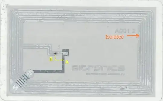
That's some plastic film with (I assume aluminum) foil wiring acting as the antenna for both powering the chip and providing radio communications.

Two things look suspicious.

First, there's a wide stripe on the right (pointed to by the arrow) - a wide carefully engineered stripe of metal not connected to anything.

Second, note what happens between points A and B which I connected with a dotted line. There's a metal stripe going from B leftwards to the card perimeter, then downwards to the end of the "tunnel" crossing the wires and that end of the tunnel is also connected to the stripe that goes to point A. So it looks like the stripe from the "tunnel" end to point B can be eliminated by simply connecting points A and B and thus saving some metal.

Why are these two seemingly useless elements of wiring present in the circuit?

suha
  • 1,774
  • 14
  • 17
sharptooth
  • 12,374
  • 26
  • 83
  • 144

3 Answers3

11

This stripe is a patch antenna, which is nothing else than a wire, printed on a PCB or similar, that radiates like an antenna.

The unconnected strip on the right is likely a reflector element, which doesn't receive any current from a direct connection but is electrically coupled with the rest of the patch to improve the radiation properties or the input impedance (these antennas are very sensitive to resonance).

While there is theory about microstrip (patch) antennas, they're not as easy as dipoles or "normal" antennas to analyze for human beings, anda great part in their design is done numerically. They can easily be considered black magic.

I'm trying to understand If AB are really connected or not:

  • at a first glance I'd say that tey are not connected, but the rounded areas are the pads to connect the ends of the antenna to the transceiver. It would be consistent with the dark path going to A.

  • Or, but this may be or may not be: some patch antennas are made of two "independent" radiating elements, of which one or both is feeded by the signal; these elements interact together like a Yagi antenna, providing a more directional radiation. So it also may be possible that there are two different loops, but it's only an hyphotesis.

clabacchio
  • 13,481
  • 4
  • 40
  • 80
  • I'm sure they are connected - the wire from A is located on the far size of the card, it goes down to the spot which connects it to the near side of the card and from there the wire goes to B. – sharptooth Jun 08 '12 at 13:55
  • @sharptooth: I can believe it, but I thought that the wire on the back was just for connecting A to the round pad in the corner – clabacchio Jun 08 '12 at 13:57
  • 1
    Yes, it connects the far sire of the thing in the center (that's a capacitor I guess) to the two round pads in the corner. – sharptooth Jun 08 '12 at 14:10
9

I will add to Clabacchio's "maybes".

As he says, the stripe at right is probably a resonant element of some sort that couples to the main loop and modifies its properties in a way that they hope will be advantageous.

The loop in the bottom left corner (shown below) will be a coupling loop that provides transformer action between the main loop and the load.

The main winding is 6 turns (it looks like 5+ but nature does not allow partial turns).
Coupling between the single turn loop (image extracted below) and the main loop gives a 6:1 voltage transformation and a 36:1 impedance transformation.
Presumably the designers found it useful to do this.
Use of an impedance transformer between a resonant circuit and a driver or receiver is common as it more easily allows high impedance high Q resonant circuits with relatively higher voltages.
The "tapping point" will be part of the black magic that Clabacchio refers to. Such designs must deal with distributed inductance and capacitance, affects on impedance of the interturn spacing and substrate material and much more. Large amounts of experience, skill, time and some luck are usually involved in quite simple looking designs.

enter image description here

ATCSVOL
  • 795
  • 4
  • 11
2

simply connecting points A and B and thus saving some metal

The amount of metal is definitely not the concern when it comes to routing traces on high frequency boards. Trace length (relative to wavelength) is very important since it affects phase shift. And loop area affects coupling.

You can't think of traces as conductors ideally connecting nodes on the circuit schematic. They are antennas, delays, resonant microstrips, inductors. A lot of RF theory goes into waveguide design.

Ben Voigt
  • 2,743
  • 1
  • 22
  • 34