2

I'm trying to analyze the Sparkfun Logic Level converter found here:

https://www.sparkfun.com/products/12009

A rough schematic is shown below:

schematic

simulate this circuit – Schematic created using CircuitLab

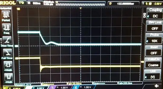
Now, I've looked at the application note mentioned on Sparkfun's page, and I understood most of it in regards to how it shifts levels, but I'm having trouble understanding the third part going from the high logic voltage to the lower logic voltage. I searched for some similar questions on the site, but teh answers that I found didn't seem to explain this part well.

My question is how does it shift the logic level from the high logic to the low logic? The app note says that when voltage on the high side, it utilizes the diode between the drain and substrate; at this point, the substrate (body) is at 3.3 V, so when the high input is 0 volts, the 'diode' conducts, dropping the voltage at the low port to 0, turning on the diode, further dropping the voltage. When the 'diode' conducts, why does it drop the source pin (connected to the body/substrate) down from 3.3 to 0? I would have thought that it stayed the same voltage at 3.3 V.

1 Answers1

3

One characteristic of MOSFETs is that the drain pin can act as a source (and vice versa) depending upon the voltages applied to the terminals. That is exploited in this circuit. When the source pin is more positive than the drain pin it will act as a drain with the drain pin acting as a source. If the source pin is more than 0.7V positive than the drain the body diode will conduct but that doesn't interfere with the FET action.

When there is a low level on the high-voltage port and the voltage between the gate and the drain pin will exceeds the threshold voltage of the device the device will start to conduct. The drain pin acts as a source pin in this case. The positive bias causes the MOSFET to conduct from source to drain and pull down the voltage on the low-voltage port down to a very low voltage (only millivolts above the voltage on the high-voltage port. I measured a BSS138 and discovered that the threshold voltage in this inverse mode is very similar to that in normal mode - I couldn't find that detail in any data sheets.

The method of fabricating MOSFETs creates the diode (referred to as a body-diode) as a side-effect - in this case the body diode does not affect operation significantly except for the case where the voltage on the high-voltage port is low enough to cause the body diode to conduct but there is not enough voltage difference between the gate and the drain pin to turn the device on - in this case the low-voltage port will be at a voltage abut 600mV above that on the other port.

As commented by @Michael Karas the threshold voltage needs to be significantly lower than the low voltage source to operate correctly.

Also as commented by @Michael Kara the physical construction of discrete devices is not symmetric but for basic analysis of the circuit it can be treated as such with the body diode in parallel.

Kevin White
  • 32,097
  • 1
  • 47
  • 74
  • Thanks for the answer. So, in this case it's due to the positive bias between the gate and the drain that causes a depletion region to form thereby allowing conductivity between source and drain, pulling down the voltage. Strange way to think about it since textbooks (at least mine) always refers to the bias between gate and source. – BestQualityVacuum Sep 18 '17 at 16:04
  • @user101402, your textbooks should be telling you about common source, common gate, and common drain configurations the same way they told you about common emitter, common base, and common collector configurations for BJTs. But they might do that pretty quickly before moving on to differential pairs and other topics. – The Photon Sep 18 '17 at 16:55
  • 1
    I think you got things a little wrong Kevin. When the high voltage side goes low it is not the Drain being puiled low which causes the N-FET to turn on. Instead what happens is that the conduction through the body diode is what pulls the N-FET source down. This increases the N-FET gate to source voltage and enables it to start to turn on. As the N-FET starts to turn on it then causes the ON FET to short out across the body diode allowing the low on the high voltage side to be seen on the low voltage side. – Michael Karas Sep 18 '17 at 17:49
  • An additional comment is that my description above should make it clear why this type of level translator circuit needs to use an N-FET that has a Vgsth that is less than the low voltage side supply value minus the body diode drop. If the FET has a Vgsth of 4.5V it does not work in this type of circuit with a 3.3V low side voltage. – Michael Karas Sep 18 '17 at 17:56
  • @MichaelKaras - No that is not correct. This circuit would work correctly even without the body diode. A MOSFET is almost symmetric in its fabrication - the terms Drain and Source are determined by the bias conditions. There are some integrated level shifters (eg LSF0204) where there is no body diode as the substrate is connected to the negative supply rail. You are correct in regard to the required threshold voltage - it can sometimes be tricky to find a device that works acceptably for 1.8V to 3.3v interface - a BSS138 is not adequate. – Kevin White Sep 18 '17 at 20:14
  • @KevinWhite: no, you're wrong. Almost ALL discrete MOSFETs are not planar, they have a vertical structure (BSS138 is vertical-structure type). Drain and source are not symmetric, like instead the MOSFETs found on ICs (LSF0204 works because those MOSFETs are symmetric). Finally, BSS138 is ok for that application (R2=10k), see output curves with \$V_{GS}=2V\$. – next-hack Sep 18 '17 at 20:58
  • @next-hack - I would consider the BSS138 marginal - 1.5v worst case threshold for 1mA doesn't give a whole lot of margin if you need a few mA to drive the load and the input drops a couple of hundred mV due it its own resistance. I agree that it will probably work (and I have had them work) but I wouldn't design it into a production device. – Kevin White Sep 18 '17 at 21:04
  • @KevinWhite I saw a lot of BSS138's (and similar) used on production devices: they are actually fine (you have \$V_{GS}=2.6V\$ just until the MOSFET turns on. Then you have 3.3V. Still 2.6V is more than 1V larger than the worst case). If you needed more than few 10's uA on that circuit, then you should either change the resistor value (10kOhm means 1V drop at 100uA), or use a more serious solution such as a level translator IC (or 5V tolerant buffer powered at 3.3V). – next-hack Sep 18 '17 at 21:10
  • @next-hack - My comment on the adequacy of the BSS138 was for a 1.8V to 3.3v application. They are ok on 3.3-5v (I have used them as such). – Kevin White Sep 18 '17 at 21:12
  • @KevinWhite Sorry, my fault, I didn't get the 1.8V! – next-hack Sep 18 '17 at 21:13
  • @next-hack - Why are you saying sorry? I saw no mention of a 1.8V application till Kevin came back and covered. – Michael Karas Sep 19 '17 at 01:26
  • @KevinWhite - I downvoted your inaccurate answer. If you were to edit and correct I would be inclined to remove the downvote. – Michael Karas Sep 19 '17 at 01:27
  • @MichaelKaras - I do not admit that your description of the operation is correct. I agree that the construction is not symmetric on discrete devices which is why from the beginning I qualified my answer by saying that they were "nearly" symmetric. If it required the body diode to operate as you describe not only would monolithic implementations not function but also it would imply you get positive feedback from a single device - no such snap action occurs. I also agree that I unnecessarily complicated the conversation by mentioning the requirements of finding devices to operate at 1.8V. – Kevin White Sep 19 '17 at 02:36
  • @MichaelKaras - I just did a simulation of a BSS123 in both forward and reverse modes (I don't have a BSS138 model but it is also a DMOS implementation). The threshold voltage seems to be identical with the two curves overlaid until the body diode prevents the drain rising further. I that case min channel would have started conduction before the body diode when driven from the higher voltage port. Admittedly this is a simulation - I have never measured the forward and reverse threshold on real devices. – Kevin White Sep 19 '17 at 03:15
  • @KevinWhite - If you research the knowledge base on the web you will find that most of them describe the discrete MOSFET level translator circuit the way I did in my comment. Even the AN10441 from the knowledgeable I2C folks at Philips (https://www.nxp.com/docs/en/application-note/AN10441.pdf) describe it this way. Your persistent stubbornness that discrete vertical FETS (with body diodes) operate the same way as lateral symmetric FETs found on a typical IC chip silicon is surprising to say the least. (continued) – Michael Karas Sep 19 '17 at 04:18
  • (continued from above) If you spend any large amount of time with simulations you should (or may have already) discovered that simulation models are often not valid outside nominal expected operating configurations. – Michael Karas Sep 19 '17 at 04:19
  • @MichaelKaras - I realize that simulations are only as good as the model. I just did a measurement on a real BSS138. I measured Vth at 100uA with Vds at 100mV. In normal mode it is 1.251v and 1.163v in inverted mode. Since the body diode has a forward drop of 625mV at 100uA it is not necessary for the body diode to play a part in the operation of the circuit. When driving from the high voltage side there will be ~600mV less Vgs than Vgd (using the real pin names). The Vgd will therefore dominate. Interesting, I had never measured that before, but assumed it. – Kevin White Sep 19 '17 at 19:37