5

I'm designing a high current linear regulator and learning about real opamps as opposed to ideal ones described in tutorials all over the net as I go.

Linear regulator schematics

My initial voltage regulation design was stable enough under the resistive load, but oscillated under capacitive load. So as I've learned on the net, I had to isolate opamp output from external capacitance and add a capacitor on negative feedback - C7. At first I've tried adding a cap from output directly to IN-, it worked, but I've noticed that when i add feedback after MOSFET output, it works better.

When I've added current limiting, the output would oscillate heavily when in current-limiting mode and the only way to stop that was to add RC network R13, C8 and a feedback cap C6 - this one worked only when I connected it on transistor output.

What I'm concerned about is that negative feedback caps are rather big, way bigger than anything I was able to find on the net as examples.

Am I doing it right?

JYelton
  • 32,302
  • 33
  • 134
  • 249
miceuz
  • 5,523
  • 3
  • 39
  • 49
  • What are C6 and C7 for? (I'm not questioning them, I just don't know) – Federico Russo May 31 '12 at 11:50
  • well, it's the core of the question - they are bandwidth limiting caps, that make high freequencies not to participate in gain. that stops opamps from oscillating. i'm not a pro, it's first time i'm stabilizing an opamp circuit, so it's just very vague and intuitive knowledge. – miceuz May 31 '12 at 11:55
  • current sense part is LTC6102 - it's current sense amplifier with current output. – miceuz May 31 '12 at 12:37
  • C6 is positive feedback, not negative. What impedance is "ISET" and "VSET"? – markrages Jun 01 '12 at 05:15

3 Answers3

11

The first rule of a control system is to never get information late. Unfortunately, this is exactly what low pass filters in the feedback path do. In particular, R13, C8, R12, C3, and C6 are going to cause stability problems in current limit mode. Also the fact the IC3B is being run open loop means the current shut off signal will slam back and forth. You are basically feeding a digital signal into a linear control loop. That is fine for something like a hard shutdown, but is not going to work for any kind of regulation.

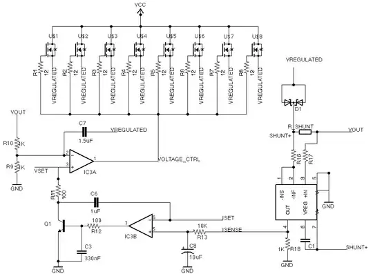
The above is assuming the mess in the lower right corner of your schematic is a current sense so that its OUT pin is ultimately a ground-referenced voltage proportional to the current thru R_Shunt. The rest of your schematic is mostly reasonable, but this mess needs to be fixed. There isn't even a component designator for that chip, let alone any indication as to what it is!

If you want to tweak the controller for good response, you need to do careful analysis. This is usually done in the S domain (Laplace transforms) looking at poles and zeros. I won't get into that here. If you want to keep it simple and are willing to give up some performance, then use the easy rule that says to make sure the controller has lowest bandwidth of anything in the system.

In voltage mode, your controller is IC3A, the thing being controlled are the FETs, and the feedback is R10 and R9. That's a straight forward system that looks reasonable except for C7. I would put C7 directly between the negative input and the output of IC3A. That effectively slows the controller. More capacitance slows it more. Eventually you reach a point where the system is stable enough. AC-wise, Vregulated and Voltage_Ctrl are close enough so that C7 still largely works where it is, but it would be better where I described. To allow for smaller values of C7, make R10 and R9 larger, like 10 kΩ for example.

On a separate note, what is D1 for? Unless you think the load can back drive this power supply, that is just a waste of a diode voltage drop.

Added:

Now that it has been clarified that this circuit is for charging a "12 V" lead-acid battery, more specific recommendations are possible.

We know the load won't change suddenly, so transient response is not a important consideration. Therefore compensating IC3A with a cap from its output to its negative input is good enough. Find the cap value that seems to make it stable and double it. The response will be slow, but again, that matters little for charging a battery.

To do current limiting, I think it would be easiest to use a separate controller with the FETs being driven by the lower of the two controller output voltages. This could be as simple as diode ORing between the two, although that would require a pullup for driving the FETs high, which would make the high and low drive assymetric. One possibility is to do diode ORing of the voltage and current mode control opamp outputs, then buffer that with a third opamp which drives the FET gates.

The trickiest part will be to make sure there isn't instability when the supply crosses over between current and voltage regulation mode. I think if each of the two controller opamps are sufficiently slowed down with a cap between their output and negative input this should be OK. Some experimentation will be required. Fortunately you are in a position to err on the side of slow response in favor of stability, so this should all be doable.

Olin Lathrop
  • 310,974
  • 36
  • 428
  • 915
  • current sense part is LTC6102 - it's current sense amplifier with current output, so yes, ISENSE is ground referenced voltage proportional to current through R_SENSE. – miceuz May 31 '12 at 12:41
  • i'm not sure about IC3B beeing open loop - it should open Q1 just enough to lower voltage on Vout to get current through R_SHUNT on the level set by ISET. I.e. it should make both inputs to be the same. But it doesn't - output really slams back and forth. – miceuz May 31 '12 at 12:47
  • yes, D1 is for protection. It's going to be lead acid battery charger – miceuz May 31 '12 at 12:54
  • olin, could you please guide me to any resource ragarding "diode ORing" all i could find is power oring, not voltage. – miceuz Jun 01 '12 at 18:40
  • 1
    You have to voltages and want to find the minimum of the two. Connect each to the cathode of a diode, tie the two anodes together and to a pullup resistor. The voltage at the anodes is the min of the two inputs plus one diode drop. Hopefully you can draw the schematic from this description (only two diodes and one resistor). The problem is that this signal may be fairly high impedance, at least for driving high. Buffering it with a opamp solves that problem. – Olin Lathrop Jun 01 '12 at 19:04
3

This system has two loops - a voltage loop based around VSET, and a current loop based around ISET. The current loop output modifies the voltage loop reference, which changes the output voltage, which changes the load current and voila, you have a closed-loop system.

If the current detection is meant as a fail-safe overcurrent protection (short circuit protection, etc.) then then IC3B should be connected to a latch circuit which shuts off your series pass MOSFETs and keeps them off until VCC is removed.

If it's meant as a soft overcurrent (i.e. to degrade regulation instead of shutting down completely), move C6 so it's between pin 6 and 7 of IC3B. I'd also get rid of C3 - if the response needs to be slower, you already have delays from R13, C8 and C6 and can adjust those accordingly.

The current loop response should be slower than the voltage loop response, so that the loops don't "fight" with each other (if the voltage loop responds slower than the current loop is reacting, the current loop output may run to saturation, which is bad news). Ballpark - keep the current loop 10x slower than the voltage loop (you've already slowed it down by adding R13 and C8, and things improved, so there you go.)

Also, C7 should be between pins 1 and 2 of IC3A - not at VREGULATED.

Adam Lawrence
  • 32,921
  • 3
  • 58
  • 110
1

You current feedback looks too linear. Not talking about caps, many of them they seem unnecessary. By linear I mean that your summation of current value and reference voltage will lead to not "current limiting mode" but just noisy feedback. Oscillations is part of this and noises. I'd try 2 things:

  • Make the current limiting more stateful so you when overload is sensed the mode can not be easily left. With linear approach the mode is "compensate the overload just enough to satisfy current sensor", which leave feedback right at the edge for a moment, then as soon as feedback comes with underload message it removes the I component from summation, and oscillation continues. Say use some non-linear component like schmidt trigger or real trigger or comparator in schmidt kind of fashion.
  • The use of voltage control path for current protection signal is adding noise. This is compromising, to reduce parts count. For reliability and cleaner design, I'd rather used current protection signal for completely separate power stage. But you have too many power transistors already, so, look if it is possible to add one diode, sink transistor and simple control directly to this transistor. It will look more like separate protection and will not involve voltage control, but just negate it, sort of override it.

You said that this project is for study. If constant current is not a first requirement mode, if it is just supplementary, then my suggestions are valid. But if you decide to redesign it completely to make it perfect, I'd say, look at the design differently.

Consider that you building a perfect current source. Design it completely, then add a voltage limiter feature just by powering U stage with independent I stage. As result you will get near perfect supply with both U and I.

  • No, the current feedback isn't linear at all. In fact it's actually in effect a digital signal, which is one of the reasons it can't ever be stable in this configuration. – Olin Lathrop May 31 '12 at 12:23
  • to make sure i understand you correctly - you mean i shoul add some hysterisis for current sense amplifier? – miceuz May 31 '12 at 12:50
  • current limiting is my primary goal too, this is going to be car battery charger. – miceuz May 31 '12 at 12:51