2

What can i do to minimize overshoot and undershoot when MOSFET switches on and off? (waveform taken using short ground spring probe, PCB is 2-layer) The rise and fall times should be less than 150ns.

Here is the picture without snubber (R1, C27) enter image description here
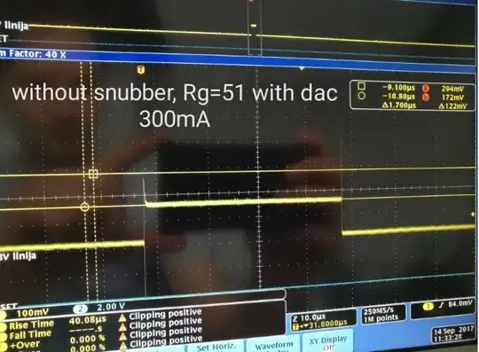
I tried using snubber on mosfet drain (3.3R, 4.7nF). Overshoot is reduced but i don't like much longer risetime..

More about schematic: It acts like a function generator: You can control frequency and amplitude of pulses. Amplitude from DAC is mixed with square signal from MCU on MOSFET Q3 drain.When amplitude is about 2V overshoot is gone. It start appear only when amplitude decreases to less than a volt. In the pictures there is about 200mV of pulse.
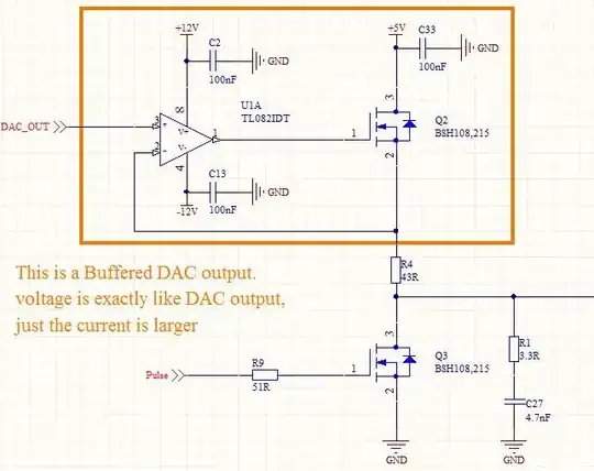
enter image description here Please suggest how to reduce overshoot and at the same time keep the edges fast (150-200ns). Thanks!
Andrius B.
  • 31
  • 5
  • Minimize inductance. Slow down turn-off. Overvoltage snubber. – winny Sep 14 '17 at 16:25
  • If your DAC is providing a DC reference level you should design your buffer accordingly. I.e. significant bulk/bypass caps at output (source of Q2) for low output-impedance broadband. Error amplifier will need compensation cap. – sstobbe Sep 14 '17 at 16:31
  • 1
    I just think that the first undershoot is due to capacitive coupling between gate and drain of Q3. The same also for the last overshoot. The first overshoot (which appears just after the undershoot) is actually much slower. And that could derive from the limited slew-rate and bandwidth of U1A. In fact, it require times to adjust the Vout according to the smaller load (because Q3 is off), and hence, the smaller Vgs-Vt required to achieve that particular voltage. – next-hack Sep 14 '17 at 16:42

2 Answers2

1

+1 for next-hack.

TL082 is a slow opamp with anemic output current. It's perfect for some other uses, but here... 3MHz GBW, 13V/µs slew rate. You shouldn't expect something with a 3MHz bandwidth to do anything useful in the 150ns time window you mention... besides, its output current is tiny, it is unable to drive a 100 ohm load, so don't count on it to push current into the capacitive gate of the FET with any enthusiasm...

Now you say this is a function generator, but it has variable output impedance: when the bottom FET is ON, then its output impedance is close to 0R. When it is off, then it is the unspecified and frequency-dependent output impedance of the bottom FET drain and the top FET controlled by the opamp.

If you intend to drive a 50R cable with this you might have problems.

Now, you got several options:

The opamp + MOSFET is a voltage regulator, and usually at the output of these, capacitors are added to clean up the transient response, because the feedback loop is not infinitely fast. Note that even with a faster opamp, you will need to carefully work on frequency compensation to make it rock stable.

Or you can kill the planet: Use a differential pair as a switch. Or two MOSFETs with complimentary drive. This throws away the current into ground when not in use, and sends it into the load when it is in use. Thus the amount of current drawn from the reference voltage is always the same, and it will have no settling issues.

Also note that you could use a smaller, faster FET to reduce capacitive shoot-through.

bobflux
  • 70,433
  • 3
  • 83
  • 203
  • Peufeu, you mensioned differential pair or using two mosfets. Do you mean using push-pull stage? Where should I put it in my schematic ? – Andrius B. Sep 14 '17 at 18:33
  • First need to know if you want to drive a cable, what's the load, etc. – bobflux Sep 14 '17 at 18:37
  • I am driving not a cable, but another opamp input. The whole circuit(not shown here) is a tansient load, and "function generator " sets amplitude and frequency of current pulses. – Andrius B. Sep 14 '17 at 18:47
  • If you're driving an opamp input, then why do you need the high-current buffer, low impedances and low-RdsON FETs? Have you considered fast analog switches or other more suitable topology? – bobflux Sep 14 '17 at 18:58
  • i haven't thought about using an analog switch. Do you mean something like this? https://postimg.org/image/img7zmwo5/ Will it be less problems with overshoots when using fast analog switch? – Andrius B. Sep 15 '17 at 05:09
  • Yes, that's the idea. This seems to be a low-current signal, so a switch with a few tens of ohms RdsON will work well, it will use very small MOSFETs, with small capacitances, so you will get less spikes. You can add a capacitor at the output of the DAC to avoid any voltage droop on switching. Make sure the switch switches quickly from one input to the other, as you don't want the input of the following opamp to be "open" for too long. – bobflux Sep 15 '17 at 14:11
  • For example, http://www.ti.com/lit/ds/symlink/sn74lvc2g53.pdf this one is quite cheap, has lowish capacitance, and switches very fast. – bobflux Sep 15 '17 at 14:13
  • I tried the chip sn74lvc2g53. The signal edges seems to be better, but ringing appeared: https://postimg.org/image/5yg0uxe1x/ How can i reduce the ringing? I tied RC snubber, didn't helped, only changed ringinf frequency. The chips is soldered with wires onto existing PCB. – Andrius B. Sep 26 '17 at 13:01
  • Well, it is better than the previous circuit! The overshoot looks more like ringing to me so I would suspect a layout issue, or ringing between decoupling caps. Since you modified the circuit a lot, I suggest you either add a huge edit to this question, or create a new question about this, and add schematics, layout, picture of the board, and any info that will help us help you ;) – bobflux Sep 26 '17 at 15:29
  • I created another thread :) https://electronics.stackexchange.com/questions/331514/fast-analog-switch-overshoot – Andrius B. Sep 27 '17 at 18:15
0

With reference to the picture below:

The undershoot is due to gate-to-drain capacitive coupling of Q3. You're bringing down the gate of Q3, to turn it off. The drain will follow it for a brief time.

The second overshoot has the same explanation. If you need to turn on the MOSFET, you'll bring the gate high. This will appear also on the drain, due to capacitive coupling.

One solution is try using a MOSFET with a much smaller Cgd.

The first overshoot is different: much slower and with a small amplitude. When Q3 is ON, the operational U1A put its output very high, so that Q2 has the required overdrive Vov = Vgs-Vth to drive the current flowing into R4 and Q3.

When you suddenly turn off Q3, the MOSFET Q2 won't require that much overdrive (it will need an almost 0 overdrive), because almost no current will be flowing. The OP amp must adjust the output, but it has a finite bandwidth and slewrate. Therefore you'll have a spike equal to Vov at the output (and it will last until the transient due to the finite bandwidth and slewrate is concluded).

For such case you might need some compensation. Or a different OP amp.

enter image description here

next-hack
  • 5,297
  • 15
  • 33
  • Thank you for detailed answer! Can you show where I should connect compensation capacitor? – Andrius B. Sep 14 '17 at 18:05
  • @AndriusB. I think it would be much easier if you used a faster OA. Still, you must then analyze the stability. By the way, what is your bandwidth you want to achieve on DAT_OUT to the output of your circuit? – next-hack Sep 14 '17 at 18:55
  • @next-hack- the output will be in the range of 10hz - 1kHz with 100ns edges. – Andrius B. Sep 15 '17 at 03:47
  • Do you want also to keep the 100ns edges? – next-hack Sep 15 '17 at 06:04
  • Yes, the edges should be 100ns, if not possible at least less than 200ns . – Andrius B. Sep 15 '17 at 06:38
  • Ok, if you want to keep your operational, and if you don't mind a continous power usage, then consider instead, as pointed out peufeu, switching the current elsewhere. For instance, add another nMOSFET (driven with an inverted version of "Pulse") that switches a 43 Ohm resistor (connected to the source of Q2) to ground. You must be careful with timings. Another way to reduce (but watch-out for power dissipation!) the overshoot, is to add an always connected dummy load (from source of Q2 to gnd). This will reduce the variation of Vov on Q2, and thus the overshoot. – next-hack Sep 15 '17 at 07:09