0

I have a resistive sensor, \$R_s\$ and I'd like to map the range \$700 \Omega - 1700 \Omega\$ to 0V-3.3V, ideally linearly.

Here's a circuit that does that (saturates slightly at low \$R_s\$ range):

schematic

simulate this circuit – Schematic created using CircuitLab

By applying ideal op-amp assumptions, the current through \$R_m\$ (and therefore \$R_s\$) is \$ \frac{V_{ref_1}}{R_m} \$

\$V_{o_1} = \frac{V_{ref_1}}{R_m} R_s + V_{ref_1} = V_{ref_1} (\frac{R_s}{R_m} + 1)\$

So the range at \$V_{o_1}\$ is 2.23V - 3.05V.

The second op-amp just scales this voltage range to approximately 0V-3.3V.

Other than using two op-amps, what are the downsides of this circuit?

Acoording to https://electronics.stackexchange.com/a/98395/2656, this task is possible with only one op-amp. Here is that circuit

schematic

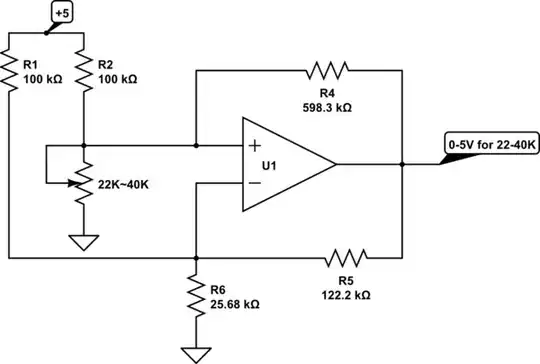
simulate this circuit (The component values correspond to a different range of voltages and resistances. Also assume that \$R_1=R_2=R_p\$. Call the sensor \$R_s\$, and instead of +5V, call it \$V_{dd}\$)

My question is: how do I analyze that circuit? I applied KCL to the two inputs of the op-amp, solved for the op-amp inputs' voltages, and set those two equal to each other, and through much messy algebra, arrived at

$$V_o = V_{dd} \frac{(R_4 R_6 - R_5 R_6 + R_4 R_5)R_s-R_4 R_5 R_6}{(R_4 R_6 - R_5 R_6 + R_p R_5)R_s-R_4 R_p R_6}$$

(V_o is not in general a linear function of R_s, however resistor values can be chosen so it is nearly linear. Perhaps there is better way to represent the transfer function so that this stands out.)

I'd like another way to reason through the circuit, perhaps relying on the symmetry of the two resistor networks at the op-amp inputs. Hopefully this way to reason about the circuit also elucidates how to choose the resistor values to map a certain resistance range to a voltage range.

Gus
  • 431
  • 3
  • 11
  • 2
    I haven't read the entire post yet, but would like to point out that \$V_{ss}\$ is typically used to refer to a negative supply, and \$V_{dd}\$ is common for positive supplies. I refer to this page on the topic: https://electronics.stackexchange.com/questions/17382/what-is-the-difference-between-v-cc-v-dd-v-ee-v-ss While you are allowed to give your nodes any name you want, sticking to standard terms will aid in communicating your design to others. This will potentially confuse a lot of people. – Joren Vaes Aug 30 '17 at 13:07

1 Answers1

1

Yes. However accurate an equation like $$V_o = V_{dd} \frac{(R_4 R_6 - R_5 R_6 + R_4 R_5)R_s-R_4 R_5 R_6}{(R_4 R_6 - R_5 R_6 + R_p R_5)R_s-R_4 R_p R_6}$$ is, it doesn't really give you a feeling for what's going on.

So let's look at the circuit, and try to get a feel for it.

R4 is big, very big. So let's ignore it to start with, replace it with an open circuit.

With R4 out of the way, and our input voltage coming from the \$R_s\$ - R2 junction (let's call that voltage and that node \$V_s\$) U1 is configured as a non-inverting amplifier, with gain controlled by R5 and R6||R1. If you want a bigger output voltage swing, increase R5, and vice versa.

R2 is quite big, it acts a bit like a current source to \$R_s\$. As \$R_s\$ increases, \$V_s\$ increases, decreasing the voltage across R2, so decreasing the current flowing through it. This would create an R to voltage non-linearity. If only there was a way of getting an increased current from somewhere to counter this happening. Wait, the op-amp voltage increases, a lot, as \$V_s\$ increases, so a small current flowing back from the output to \$V_s\$, through a big resistor, will do the trick.

What value should R4 have? If I change R4, then \$V_s\$ will change, and the output will change, so we need a closed form solution for it? Not necessarily, the effect on \$V_s\$ is small. Compute the current in R2 for two different \$R_s\$ values, and pick an R4 to keep the R2 current constant. Now recalculate with the new values. It will converge in a few steps.

R1, what's that doing? With R6, it's setting the voltage about which the U1 non-inverting amplifier is amplifying. So if you want a different output offset, change the R1 to R6 ratio.

That's how I'd analyse the circuit. And then I'd whack it into a simulator like LTSpice, and trim the resistors onto obtainable E24 or E12 values.

Neil_UK
  • 158,152
  • 3
  • 173
  • 387
  • Thank you for these insights! You mention that the non-inverting amplifier gain is given by R5 to R6||R1. If R1 were infinite, the expression for the gain would be (R5+R6)/R6, which doesn't match what you wrote. In general, it is (R5*R6 + R1*R5 + R1*R6) / R1*R6 Thanks for explaining how to pick R4. Is it the R that is picked last? Also is there a reason that R1=R2? – Gus Aug 31 '17 at 01:37
  • 1
    when I said 'given by the ratio', I wasn't saying 'equal to' but 'dependent on', however I've edited my answer to remove that ambiguity, your expression with R5 and R6 is correct. The inverting side R1, 5, 6 and the non-inverting side Rs, 2, 4 are completely independent, the nodes they meet at are low impedance (5v and the amp output). This means that only the ratio within each side affects the operation, so R1 and R2 can be chosen independently. An observation, *all* engineers run out of 1k, 10k, 100k resistors in their resistor packs first, because they all pick easy values. – Neil_UK Aug 31 '17 at 06:36