The FDC855N comes in a 6-pin package, 4 of which are connected to the drain, and only 1 to the source. Why this difference? The source sees the same current as the drain, doesn't it?
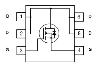
The FDC855N comes in a 6-pin package, 4 of which are connected to the drain, and only 1 to the source. Why this difference? The source sees the same current as the drain, doesn't it?
That's not for the high current, it's for heat management.
The single source pin can handle the current, and so would a single drain pin. Schematically a MOSFET is often drawn symmetrically, because this way it's easier to show the asymmetry in the channel's conductivity.

But discrete MOSFETs aren't constructed that way. More like this:
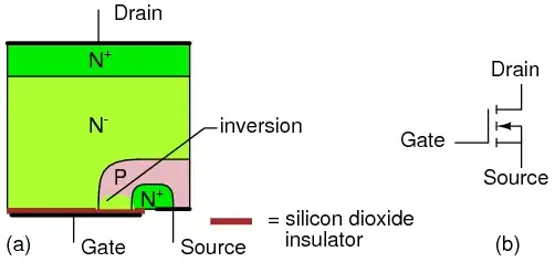
It will probably be packaged upside down, with the bulk of the drain connected to the lead frame which directly connects to the 4 pins. Gate and source will be bonded to their pins.
The bulk of the MOSFET will dissipate the most heat, and because its direct contact with the pins the heat can be drained through the pins, it's a path with low thermal resistance. The drain may still be wire bonded as well, for proper electrical connection. But the bonding wire will pass much less of the heat.
Thermal resistance in conduction (to the PCB's copper) is much lower than that of convection (the way heat is exchanged with the air above the package). I found the following suggested pad layout for a Luxeon power LED. They claim it can easily achieve 7K/W.
In SMT power MOSFETs which will have to dissipate quite some heat it's advisable to have the drain pins on a larger copper plane, or allow the heat to dissipate through a series of (filled) vias, like for the Luxeon LED.
This will be for cooling purposes - you will notice on the bottom of page 2 they make a big point that the way copper the pins are connected will change the thermal characteristics. Most of the heat goes through the pins and not the package to air.
This quite common - the IRFD9024 has two pins for the drain and explicitly mentions "The dual drain serves as a thermal link to the mounting surface for power dissipation levels up to 1 W"
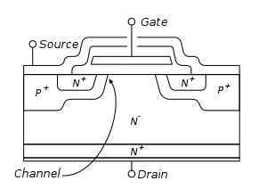
This is particularly common with HEXFET and PowerTrench power MOSFETs as the drain is connected to the bulk of the substrate, and the source is a metallic layer on top. The drain is more closely thermally coupled to the substrate, so is better to remove heat.
Most power MOSFETs are classified as vertical-diffusion MOS as compared to the planar or lateral MOS used elsewhere. This is largely because to maximise current carrying capability, you need an extremely long but narrow channel, which is hard to do using the textbook symmetrical MOSFET. The exception to this will be power MOSFETs designed for audio amplifiers - these are lateral MOS and you will usually find that they are conventionally heatsunk a a result.