6

Disclaimer: I only have about 2-3 months of semi-intensive electronics experience.

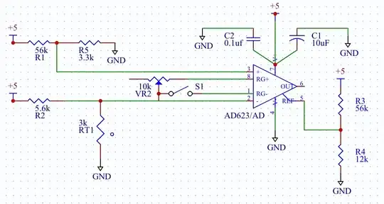
Note that the chip (to the left of the Arduino, is Analog Digital's AD623 Instrumentation Amplifier) Datasheet here.

Note that the Potentiometer VR2 sets the gain in the circuit (according the the AD623 datasheet I should be getting a gain of around 5).

The thermistor (RT1) I am using is just a normal NTC thermistor that is quite stable.

I am having the following problem: The voltage I am reading between the Output of the AD623 and the Arduino Ground (The same as the REF Pin of the AD623) seems to fluctuate in a not random but unusual way.

It used to jump around wildly but I re-soldered some connections and that seems to have gone away, what I am seeing now is the slow drift over a range of 1-2 volts of the signal. (Note I am trying for a dynamic range of about 4 volts, so this is quite large). It is almost as if the Instrumentation amplifier just has a really really bad slew rate. Then once it seems to have settled it slowly moves on (randomly) up or down by about a volt the same way, this then repeats.

I realize that this is very similar to the thread voltage fluctuations in Arduino opamp thermistor circuit (I do in fact work with that OP - on a somewhat different problem), and I found the answers to her question very unhelpful.

I have considered that this drift could be something as trivial as room temperature and air currents but my reference thermometer often (but not always) seems to track inversely (and other times somewhat linearly) with the voltage I read between the output and ref.

I do not so much care what the relationship is between the voltage read between the AD623 output and ref as long as that relationship is constant, so that I can calibrate it and trust that the calibration will give me the correct temperature when I read off the voltage.

UPDATE: With everyones help (Especially Olin Lathrop) I think the problem has been fixed. I had been trying to use the AD623's 2 inputs to compare the resistance of a thermistor (RT1) to the equivalent resistance of the thermistor at room temperature. (Making VR1 look like RT1 at Room temperature) (circuit shown above) The problem was that I had my REF output from the AD623 tied to ground. However what I was actually doing was trying to set VR1 so that the voltage between OUT and REF would be just above the bottom supply rail. NOTE: This is not equivalent to making VR1 look like RT1 at Room Temperature. I did this to maximize the dynamic range of the output, however in doing so I also had to increase the gain (set by VR2). Such a high gain amplified the internal voltage offset of the AD623 (This voltage offset can itself fluctuate, leading to the symptoms I described above).

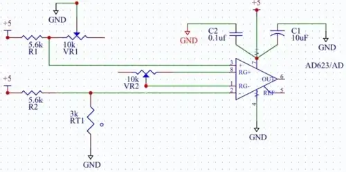
That said here is the schematic that seems to be working for me (compare to the starting point above).

enter image description here

jds
  • 235
  • 1
  • 2
  • 8
  • As was already pointed out in your last question, that is not a schematic. It shows what pins are connected to what, but does not show the circuit. Post a real schematic. No excuses. This is getting tiresome. If you don't have a better diagram, make one already. – Olin Lathrop May 22 '12 at 23:36
  • 3
    Olin: OP posted a link to the JPG (not a great schematic but it's good enough for this purpose) but can't post images yet due to lack of reputation. – Jason S May 22 '12 at 23:54
  • @OlinLathrop I have added my best attempt at a schematic (above) here is the link: http://justin-silverman.com/AD623Therm.png Again I do not have enough reputation to post it directly. Thank you again for your help. (I found some Web site online that let me do this for free, if you have a better suggestion I would welcome it). – jds May 23 '12 at 00:36
  • I added the second schematic image. – Connor Wolf May 23 '12 at 03:15
  • Did you ask the question under a different account first justin? – Kortuk May 23 '12 at 14:50
  • @Telaclavo Yes you are very right, I appologize, Olin Lathrop pointed this out and I have fixed the schematic (removed the "wiring diagram") – jds May 23 '12 at 15:16
  • @Kortuk I do not think so... – jds May 23 '12 at 15:17
  • Your new schematic link results in "403 Forbidden". This is getting ridiculous. I'm close to thinking this question is irreparable and needs to be closed. – Olin Lathrop May 23 '12 at 15:43
  • @OlinLathrop I am so sorry, this is really not my day. I just fixed it. – jds May 23 '12 at 15:46
  • 2
    Connecting potmeters like this is a Bad Habit™. If the wiper makes a bad contact (it's a mechanical thing!) the resistance will go to infinity. Connect the open end to the wiper. If the wiper then makes a bad contact the resistance will be limited to the potmeter's total resistance. – stevenvh May 23 '12 at 16:13
  • @stevenvh Thank you, what should I connect it too? – jds May 23 '12 at 16:14
  • Like I said: the open end to the wiper (the end with the arrow). For VR1 you connect the open end at the right to GND. – stevenvh May 23 '12 at 16:17
  • When this does get worked out to a functional point will someone flag me to come clear out the useless comments about improving it? – Kortuk May 23 '12 at 16:22
  • @Kortuk Flagging you to clear out comments. – jds May 24 '12 at 23:40

1 Answers1

4

For reference, here is the schematic you supplied that we will be discussing:

There are many things wrong here:

  1. Use component designators. Lack of proper designators makes it hard to talk about individual components.

  2. The two bypass caps are doing nothing. It is a good idea to use bypass caps, but they need to be between power and ground and close to the chip. You should have been able to see for yourself that the two caps are shorted.

  3. Both inputs are effectively held at ground, so the output will be independent of any temperature sensor, which doesn't seem to exist anyway.

  4. The two extra floating connections on the positive input and one extra floating connection on the negative input don't do anything useful unless you are trying to pick up noise.

  5. The gain is unpredicatable and not guaranteed to be bounded to valid values for this amp. With the 10 kΩ pot there, the gain can be from 11 to infinite. I would do experiments with a fixed known gain resistor. Right now you don't know what you have. Initially you could even leave off the gain resistor to get a stable gain of 1. Make sure everything works, then try a higher gain by using a fixed resistor.

I'm guessing the most likely cause of your symptoms is you have the gain pot cranked to invalidly high gain, so the output is small input offset errors amplified. These can come and go and possibly oscillate as different parts of the chip heat or cool slightly from other parts of the chip.

Fix all the things mentioned above before coming back with more questions. Next time I won't be as forgiving of obvious sloppiness and bad schematic drawing. When you are presenting things to others, it's your job to present them clearly and neatly else risk being dismissed as a waste of time.

Added:

You have now revised your schematic:

This looks like a more reasonable bridge circuit, but you still haven't fixed the basic problem of possibly having invalid gain. I don't like having to repeat myself. Replace VR2 with a fixed resistor, or leave it off to get unity gain for initial debugging.

With a reasonable value for VR2, you should be able to vary VR1 and watch the output go up and down over part of the range of VR1. When VR1 is close to the value of RT1, the two inamp inputs will be close to the same value. If REF is tied to ground, then you'll be right at the edge of a output response. It would make more sense to tie REF to 2.5 V so that the output is at mid range when RT1 equals VR1. You should then be able to see the output go up and down as you heat and cool RT1.

Olin Lathrop
  • 310,974
  • 36
  • 428
  • 915
  • I am very sorry for the mistakes. I have read your post at: http://electronics.stackexchange.com/questions/28251/rules-and-guidelines-for-drawing-good-schematics And tried to implement all these points (updated above) In short I _think_ I have fixed your points 1-4, With regards to 5) I will try this right away thank you! – jds May 23 '12 at 15:18
  • With the gain set to 1 (by adding a switch in the off position between RG- and VR2) I still see the same "drift problem" I describe above, just now at a much lower voltage. Could this happen if I had damaged the chip? I have two of them and get the same problem with each, (I could have damaged both I guess... Not sure how though) – jds May 23 '12 at 16:09
  • 1
    Thank you very much for all your help, After nearly 2 months debugging this from what was an even more embarrassing design, I have a working product. Sorry for the difficulty, I really appreciate the help. – jds May 23 '12 at 22:12