Consider DDR, PCI, etc. There are various signals, plus a clock.
You'd like the signal that says "this data is valid" to arrive when the data is actually valid. Also all the bits should arrive at the same time. And everything should be properly aligned relative to the clock.
- Source Synchronous (HDMI)
This is similar, as you have a few data lines synchronized to a clock. (see below).
In this case, there is no clock, so the length of the cable does not matter. However you still have a:
Both halves of a differential pair radiate and pick up the exact same amount of noise than a single wire or PCB trace would. Since both halves carry exactly opposite signals, the radiated fields cancel, and as a result the overall radiated noise is very low. Also, the receiver can reject the common mode noise that is picked up by both halves of the pair.
However, if the lengths of both halves are unmatched, this no longer works. Noise which is picked up will appear first on one half of the pair, then on the other. It is no longer common mode, so it cannot be rejected. Also, if one line is longer than the other, the signals in each half will no longer be opposite, one will be delayed. So the emitted EM fields will no longer cancel, and it will radiate noise.
The clock is the most important. Usually, the device will latch in the incoming data on a clock edge: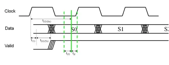
Now, data changes from "S0" to the next bit "S1" then "S2", etc. In this example, data is latched in on the clock rising edge. So you want the clock rising edge to be right in the middle of each bit. This ensures maximum robustness to variations in timing towards one side of the other. (Depending on setup/hold times, the optimum may shift a little bit).
Both RAM and CPU can send signals on the same data bus. Back in the old days, everything would use one single clock. This simple scheme has one drawback: roundtrip times. Consider this:
- Clock goes low
- Clock propagates from clock generator to RAM chip
- RAM receives clock edge, then outputs a bit (this also takes some time)
- Bit propagates from RAM chip to CPU
In this scenario, the clock used by the CPU to read the data sent by the RAM is the main clock... so, the propagation time from the clock generator to the CPU should match the propagation time of the whole sequence above, includes the RAM chip's response time. This is a mess, and the reason why busses like PCI were limited to rather slow frequencies.
If you want high-throughput, then the clock has to be generated at the source of data, and sent along with the data, on length matched traces. This eliminates the need to synchronize everything to a distant clock chip.
This is why SDRAM (SDR, DDR, etc) uses two clocks. The CPU sends its clock and data. When the RAM replies, it also sends its own clock along with the data. Both clocks have the same frequency, but different delays. Usually the slave chip needs a PLL to regenerate the clock while adjusting its phase relative to main clock, in order to compensate for variations in propagation times due to different chips, boards, temperature, aging, etc.
Every modern high-throughput link uses one of two schemes:
- Embed clock into data (SATA, PCI-Express, USB, Ethernet, etc). In this case, different parallel lanes may not need to be length-matched.
- Both sides transmit in source-synchronous mode (data+clock) to allow a clock faster than the roundtrip delay (SDRAM,DDR,etc).
Matching trace lengths is only part of the story. Drivers and receivers delays do vary with temperature, and chip to chip. This is called "skew". For example a 8-bit parallel buffer will specify a skew, which is the difference in propagation times between each individual buffer in the chip.
