A common rule of thumb you hear when learning Electrical Engineering is that the gate current of a MOSFET is always approximately 0. When is it not safe to assume that it is 0?
Asked
Active
Viewed 5.3k times
20
-
A FET gate may have a pull-up/down resistor, by design drawing more than the gate leakage current. – tyblu May 10 '12 at 11:12
6 Answers
27
Under transient conditions, the gate current will be non-zero since you need to charge (or discharge) the gate capacitance and this requires current. The larger the gate current, the faster the gate voltage changes and the faster the device switches. Once the switch transition is completed, then the gate current approaches zero (and is mostly the leakage current).
For low switching (PWM) frequencies, the rms gate current will be low. Higher switching frequencies will increase the rms current.
madrivereric
- 1,664
- 9
- 10
-
1All aspects of this answer impart a very strong sense of deja vu :-) – Russell McMahon May 10 '12 at 09:05
-
"Higher switching frequencies will increase *the average of the absolute value of the current*". The average current is independent on the frequency. – Telaclavo May 10 '12 at 09:47
-
1All aspects of this answer impart a very strong sense of deja vu :-) :-) – Russell McMahon May 10 '12 at 12:46
-
@Telaclavo - The average current will be independent of frequency on any sufficient period of time, because it is (ideally) zero. Any non-zero value will mean charges are built up continuously and a gate cannot store an endless supply of charges. The absolute value however, is not. Higher frequencies imply the same charges are being moved to and from the gate at a higher rate, i.e. a higher absolute current. – Marcks Thomas May 10 '12 at 14:21
-
20
The most important exception is usually not static leakage but when charging or discharging the gate capacitance to turn it on or off.
Gate currents of around 0.1 to 1 amp are typically required to charge and discharge the gate capacitance in usefully fast times.
Too fast leads to extra losses.
Too slow leads to FET being in active resistive state between off and hard on and dissipating very substantial amounts of energy relative to what can be achieved with proper design.
This is why gate drivers are required and why you cannot just drive a MOSFET gate at high frequencies from a microcontroller pin typically able to deliver 1 to 30 mA, even when voltage requirements are well met.
_______________________________-
Related - MOSFET gate drive currents:
It is often not appreciated that a MOSFET being switched at 10 kHz plus may need gate drive currents on the 0.1A - 1A range to achieve adequate switching times - depending somewhat on application. At many 10's of kHz gate drive at the higher end of the range would be common.
MOSFET datasheets specify gate charge and gate capacitance. Capacitances are typically in the "few nanoFarad" range and gate charge is typically a few tens of nanocoulombs and input capacitance is typically a nanoFard or few.
Using Digikeys parametric selector I just subset N Channel MOSFETS of 60-100 V Vds and 10-20 Amp Ids.
Gate charge was as low as 3.4 nC and input capacitance = 256 pF and
as high as 225 nC with 5700 pF input capacitance
with bottom median quartile = 18 nC and 870 pF and
top median quartile = 46 nC and 1200 pF
That charge has to be "pumped" into and out of the gate capacitance.
If you are PWMing at say 10 kHz then 1 cycle = 100 uS so you'd hope that switching times were a small fraction of that. If you want to charge or discharge a few nF to/from zero to typically 3V to 12V then having at least 100's of mA of drive is a necessity.
1 Coulomb = 1 amp.second so 10 nC requires 1 A mean for 0.01 uS or 0.1A mean for 0.1 uS. The horrendous outlier MOSFET above with 225 nC gate charge would take 0.225 uS to charg at 1A and 2.25 uS at 0.1A. The reason that this FET is so much worse than most is that i is "sepcial - it's a 100V 16A depletion mode device that is usually on with no gate voltage and requires negative gate voltage to turn it off. However, one can still be "caught out" by eg this 60V, 20A part with 100+ nC gate charge.
This more normal 60V 14A part has 18 nC max gate charge. Drive it from a microcontroller port pin at 10 mA and it will take ! 1.8 uS to charge the gate capacitor - probably acceptable at 10 kHz and very bad at 100 kHz. With rise and fall switching times of 110 and 41 nS when 'properly driven' you'd want rather better than ~ 2 uS gate charge times to switch it anywhere near its upper limits.
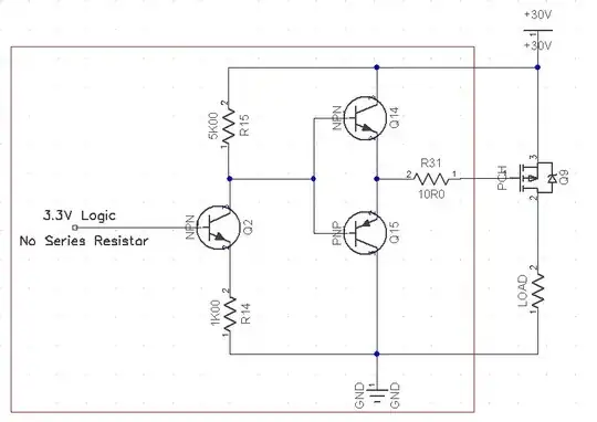
Example:
200 nS high-side gate driver:
Source of this circuit not certain - via PICList member I think. Can check if anyone cares. Note hat this circuit is considerably more "clever" than may be apparent. (Olin is fond of the input arrangement used here). The ~= 3V swing across R14 causes an about 15V swing about R15 so Q14/Q15 bases swing from +30V to about +15V, providing ~ 15V if high side gate drove to the P Channel MOSFET.
Russell McMahon
- 147,325
- 18
- 210
- 386
-
1Which type of MOSFETs are you describing? (Re: "...typically required...".) – tyblu May 10 '12 at 11:31
-
@tyblu - Almost any sort of power MOSFET switching more than trivial currents. Say a few hundred mA on up. Look at data sheets for gate charge and gate capacitance. That charge has to be "pumped" into and out of the gate capacitance. If you are PWMing at say 10 kHz then 1 cycle = 100 uS so you'd hope that switching times were a small fraction of that. If you want to charge or discharge a few NF to/from zero to typically 3V to 12V then having at least 100's of mA of drive is a necessity. – Russell McMahon May 10 '12 at 12:51
-
Ah, power FETs. Am used to <500mA Ids, where input is <1nF. Note that datasheet stated gate capacitances are always at a certain frequency (eg. 1MHz). – tyblu May 10 '12 at 18:29
-
So when there is 3.3 V at the base of Q2 its emitter voltage is about 3.3 - Ube = 3.3 - 0.7 = 2.6 V and Ic = Ie = 2.6/1k and the voltage accross R15 is Ic*5000 = 13 V and the voltage at the bases of Q14 and Q15 is 30 - 13 = 18 V meaning Q2's Uce = 14.4 V? And then the voltage at Q14's emitter is 18 - Ube = 17.3 V? Is there a similar schematics for driving the low side N-channel MOSFET? – Chupo_cro Jul 27 '23 at 21:58
-
1@Chupo_croLow side can usually be driven with just Q14 and Q15 driven by low current drive input. Or as shown but with R14 removed, a Q2 base resistor dded and Q14 driven from a suitable supply voltage - possibly a dropper resistor from +30 and a zener and large enough filter capacitor. || Or you could use this circuit but provide R15b in Q2 collexctor so that Q14 base swings high only to an allowd voltage. || OR ... . – Russell McMahon Jul 29 '23 at 10:40
-
Author of [this project](https://tinyurl.com/5n9xynk4) linked to your schematics as a start point for his version of low-side 32kHz PWM 5V driver for IRFZ44N at 24V which is not good because max Vgs is only about 4.3V and Zener diode does nothing. I tried to modify your shematics, do you think [this](https://tinyurl.com/2de3kd56) would be reasonable? Seems as it could work, Vgs is over 10V but the base current of the PNP transistor (the 2nd from the left) is almost zero. In [this project](https://tinyurl.com/2s3u35jt) he used your schematics but added a Zener diode which I think is not needed. – Chupo_cro Jul 30 '23 at 19:56
-
1@Chupo_cro Ask again in 3 days time. Criticalproject happening. I think yours may be better doing inversion (if neded) at imput so high voltage switching concentrates on driver task only. ie move your Q2 (2 from left) to left side to invert. || Where are his links to my diagraam - I cant see them. || His IRFz44N has Vgsth of 2-4 V so MAY work OK in some cases. He also needs a front end level increaser (one more transistor). | A pulled high diode or two may be enough. (Very Heath Robinson :-) ). eg R to 30V pulls up diode(s) to Vin with mybe zener clamp. A trnsistor is easier. || Later. – Russell McMahon Jul 31 '23 at 03:02
-
He linked to this topic under **The soldering iron heater** paragraph in the sentence "This forum thread explains the problem in details." - the word "This" is the link. If you open the link I posted before with Chrome, the paragraph title will be highlighted. He apparently used your schematics but made a mistake when trying to convert it for N-channel low-side MOSFET. Yes, Vgs(th) is max 4 V but Rds(on) is 22 mOhm only when Vgs is above 10 V (and under 20 V). In my schematics there should be 14 V swing at the gate. You can flip the switch and check the voltages with the mouse cursor. – Chupo_cro Jul 31 '23 at 03:25
-
1@Chupo_cro Yes. " ... MAY ..." :-) :-(. || Something to try for now. Input transistor with base via R to say 3V3. Drive emitter with Vin. Collector to some Vhigh. This gives a non inverting high swing drive at collector. Cn be zener clamped if desired or whatever else suits. || Later ... – Russell McMahon Jul 31 '23 at 03:32
-
I'll try to find some solutions in the next few days. The final solution should work with 5 V signal and 24 V supply for the heater. In his [next project](https://www.hackster.io/sfrwmaker/soldering-iron-controller-for-hakko-t12-tips-on-arduino-f7a888) for the very same soldering iron he used the exact your schematics without changing the resistor values (this time he used P-channel high-side MOSFET) but then the voltage swing at gate was to high and he used a Zener diode. But I think it is enough to only replace the 5k resistor with 2k7 like [this](https://tinyurl.com/26jyafnw). – Chupo_cro Jul 31 '23 at 03:40
12
Check the datasheet. For this MOSFET they specify a gate to source leakage current of maximum 100nA. If you're driving the FET from an opamp, for example, you can probably ignore that. If you're using some static voltage with a very low charge the 100nA may be too much. It all depends on your application, but in most cases this static current will be negligible. Switching on and off will cause a much larger current peak to charge and discharge the gate's capacitance.
stevenvh
- 145,145
- 21
- 455
- 667
2
Hypothetical situation: say you wanted to implement instrumentation/sensing of voltages generated by very tiny charges. (Charges that could be drained by even a tiny current through a very high impedance.)
Kaz
- 19,838
- 1
- 39
- 82
-
Yes, and I needed to measure microamp-level quiescent currents in test equipment. Turns out the 100nA can be ignored, but I didn't know what to expect until @stevenvh gave us a real-world typical value. – gbarry Sep 24 '20 at 21:59
1
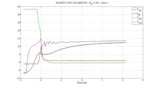
Here are some waveforms that indicate some of the transient natures of a large MOSFET. The gate current gets high during switching and may have caused a dip in the gate drive voltage here. (black line)
 .
.
Tony Stewart EE75
- 1
- 3
- 54
- 182
-
3Gate current is one of the things not shown in that graph, is it? And what is \$V_{GG}\$? – Telaclavo May 10 '12 at 10:18
-
1
0
I think this generalization comes from comparing a MOSFET to a BJT in terms of an idealized amplification application.
"A BJT is a current-controlled device (base current controlling collector current, base voltage clamped to a PN forward drop) whereas a MOSFET is a transconductance device (base current is negligible, base voltage controls collector current)", as the teacher says.
When you're talking about "steady-state" amplifiers (no hard switching or large swings in biasing) the assumption of 'zero base current' holds true enough to allow you to do meaningful work.
When you introduce high-frequency hard switching, as others have pointed out the inherent capacitances of the MOSFET dominate the behaviour (i.e. the base current drawn is a function of charging and discharging the gate capacitance) so the 'zero current' assumption is invalidated.
Adam Lawrence
- 32,921
- 3
- 58
- 110