14

When driving inductive loads with transistors, we use kickback diodes.

What I understand is a kickback diode supplies a path for the inductive charge to discharge. Also, an inductor will try to resist the change in the current, turning into something like a voltage source that will source the current in the same way it was before, in case of a break in the current (for example when the transistor turns OFF).

In the below circuits, there are two different placement of the kickback diode. D1 is placed in a logical way, so that the charge in L1 will discharge through it, protecting Q1's collector from over-voltage or breakdown.

However, the second circuit with D2 makes no sense to me. How can D2 prevent any damage when it is reverse biased? I was seeing this configuration rarely, however I saw it in a Lenze driver schematic and couldn't understand it.

How does D2 prevent any damage due to inductive kickback?

Kickback diode configurations

abdullah kahraman
  • 5,930
  • 7
  • 59
  • 104
  • 4
    Are you sure D2 wasn't a zener? – Federico Russo May 01 '12 at 15:28
  • Nope, it was a normal silicon diode. – abdullah kahraman May 01 '12 at 15:41
  • 1
    Almost certain this is a dupe of one I answered in the past. Ah, here it is: http://electronics.stackexchange.com/questions/26944 – markrages May 01 '12 at 16:50
  • On a side note: 1N4001 is a bit slow for this application. I usually see 1N4148. – jippie May 01 '12 at 16:58
  • 3
    @jippie: 1N4001 can handle significantly more current than 1N4148. 1N4001 is indeed slow to turn off, but this is not a issue if the inductor is only turned on after a long enough off time to ensure the diode is no longer conducting. From the limited information given, you can't say that the indicated diode is inappropriate and 1N4048 would be better. – Olin Lathrop May 01 '12 at 17:27

3 Answers3

11

Just to point out one thing.

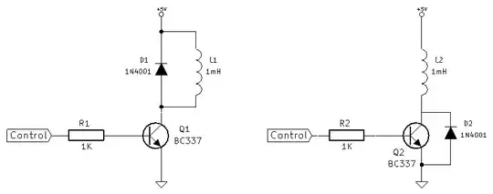
Assume D1 is not there. You wrote:

turning into something like a voltage source that will source the current in the same way it was before

No. Don't think of it that way. Inductor L1 does not turn into anything else, when Q1 opens. In fact, L1 does not even "see" outside of it. It just sees its current, and the differential voltage across its two nodes, and keeps them coupled, so that the physics law it is programmed to perform (\$v=L\dfrac{di}{dt}\$), gets performed always. If a circuit was a multicore machine, each part (in the lumped model) would be a single-core processor executing always the small piece of code it would be programmed to run, without knowing anything about the other parts.

When Q1 opens, inductor L1 continues obeying the physics law it is programmed to obey, and that implies that, assuming finite voltages and currents (as it is in real life), its current can never have a discontinuity. That means that the current through L1, right after Q1 opens has to be exactly equal to the current through L1 that existed right before Q1 opened. The inductor just continues doing its "task". What has changed is not the inductor. Is Q1. Now Q1 is an open circuit. So, that current that continues flowing trough L1, where does it go? There is no D1, and Q1 is open. Well, it goes to the parasitic capacitance (\$C_c\$ in the drawing) that exists between the collector of Q1 and ground, and charges it. That parasitic capacitance is very small but VERY real. There is no way to make it zero. It is not shown in your schematic, but just because that's a simplified schematic. The real schematic should show this real parasitic capacitance, and many more things. Now back to it being charged. Since it is a very small capacitance (it may be well below 1 pF), that means that even a small current will charge it very quickly , and up to many volts, due to \$v=\dfrac{1}{C}\int{i·dt}\$. The current through L1 is not even a small current. It's usually a "normal" current, or even a high current. That means that the parasitic capacitance \$C_c\$ may be charged very quickly, and up to many volts. Even many thousand volts. And that's what may destroy Q1.

But the most important thing is that there is no "magic", in electronics. Nothing turns into anything else. The inductor always behaves as it is "programmed" to behave. It never turns into something like a voltage source. It's the existence of that unavoidable parasitic capacitance \$C_c\$ what explains easily why voltage builds up at the collector of Q1 (and why some means to avoid that are needed).

enter image description here

Telaclavo
  • 4,867
  • 19
  • 28
  • 1
    You explain why some form of protection is needed. But you don't explain how D1 achieves this, and neither do you talk about the D2 solution. – Federico Russo May 02 '12 at 14:09
  • @FedericoRusso he points out that one thing that I wrote was wrong. Telaclavo you are right, and I knew I was wrong, I just wanted to be more understandable and simple. Thanks for the answer, I didn't know it was flowing through the parasitic capacitance. – abdullah kahraman May 02 '12 at 14:18
  • 1
    One problem with the "multi-core machine" analogy is that computers implement unidirectional cause/effect relationships. An inductor is more like a flywheel (current==speed and voltage==torque); applying torque to the shaft will change the speed, and external efforts to change the speed of the shaft will cause the inductor to apply torque in a continuous bidirectional cause-effect relationship. – supercat Apr 01 '13 at 15:13
  • Even if there were no parasitic capacitance associated with the transistor, just the big voltage spike developed by the diligent inductor,trying to be a good inductor, could easily be high enough, just as a voltage, to break down the now "turned off" biasing of the semiconductor internals, and allow current to "break on through to the other side" and let (I^2)*R cook things from there. I'm just nitpicking, by saying the voltage alone might break down the now insulating semiconductor junctions down. They'd probably be working together, helping each other blow up poor Q1. Two transistor terroris –  Mar 21 '14 at 01:20
7

The first circuit D1 is correct in that it safely deals with the inductive kickback.

The second circuit makes little sense on its own. As Federico pointed out, D2 could provide a safe path for the kickback current it if were a zener, but it's not a shown as a zener and a 1N4001 is definitely not a zener.

D2 might make sense if L2 is more than just a inductor and could externally be driven backwards. That could be the case if it is a motor winding, for example. In that case D2 clips negative voltages before they can harm Q2, but it does nothing to safely limit inductive kickback when the transistor is turned off.

Olin Lathrop
  • 310,974
  • 36
  • 428
  • 915
  • 1
    The zener configuration will make the current travel through the ground, back to the supply, creating a bigger loop and may create a significant ground bounce if switching current is high enough, where the first circuit with D1 deals with very small loop area and does not have a current flowing through ground, right? – abdullah kahraman May 01 '12 at 20:09
  • 4
    @abdullah: You are right about where the currents flow, but there shouldn't be much ground bounce with a zener because the same current was originally running to ground thru the transistor before it was switched off. – Olin Lathrop May 01 '12 at 23:00
  • 2
    @OlinLathrop: By my understanding, using a Zener as shown should actually reduce ground bounce and supply disturbance, since with a flyback diode on the coil the supply and ground currents would almost "instantly" drop to nothing when the transistor switches off, whereas with the ground-wired Zener they would ramp down to nothing as the inductor's energy is dissipated. On the flip side, any supply current which is drawn during that time would represent extra energy that would have to be dissipated (wasted) in the zener. – supercat Apr 01 '13 at 15:18
0

Because the diode conducts during counter emf. The counter emf voltage is opposite from the applied voltage, so the diode goes into forward bias in that moment. Either way is ok, the second one is usually used to express the circuit in a coil driver transistor like a tip122 transistor

drtechno
  • 1,033
  • 6
  • 8