3

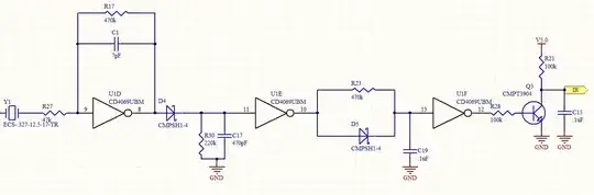
This is a follow up to an earlier post I made here. Below is the relevant portion of the schematic for this issue (stuff to the left of Y1 is in original post if necessary).

Schematic

I have finally gotten this circuit working somewhat reliably with one exception. The original device (read layout) is intended to work at 5V. I have the original device and can verify that it does work properly at 5V. I just got my PCB back which has a copy of the circuit. I populated the board and fired it up and it seemed to work like a champ. I had both (original and copy) wired up on the bench and was looking at the output of each channel on the scope. Things looked great.

Then, I happened to notice that I was powering up the two from 3.3V as I've been switching between projects and did not change the power supply voltage when I last switched. I begin to adjust the voltage up toward 5.0V and I notice that right about 3.8V the output of the copy goes low and stays low up to 5.0V. I lower the voltage and it goes high (but toggles low when IR present) at about 3.6V. So, the circuit works at a supply voltage < ~ 3.6 V.

With the voltage set at 5.0V I start to probe around comparing all signals to the original. Following the individual inverter stages things look identical right up to the input of U1E (pin 11). As I vary the voltage across that threshold of roughly 3.6V that pin toggles. So, next I want to take a look at the output of U1D (pin 8). I found it quite difficult to probe this and watch the scope at the same time as the probe would slip off the contact point. So, I decided to take a piece of 3" wire wrap and tack it onto the pin so that I could grab a hold of it with the probe. I did that, fired it up and the circuit behaves quite nicely! It operates as expected. At this point I don't even have the probe on the wire I tacked onto the pin. So, the addition of this wire hanging from the pin has solved my issue.

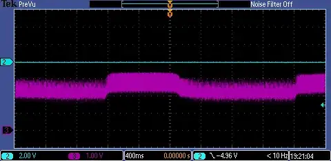
I have two screen shots of the oscilloscope. The first is the screen shot with no wire tacked on to the output of U1D.

Misbehaving

The second is the screen shot with a wire tacked to the output of U1D.

Behaving

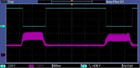
The blue trace is the output of the entire circuit (Q3 Collector). The magenta trace is the input of U1E (or cathode of D4). You'll notice I gave each two pulses from the transmitter. In the snapshot without the wire tacked you'll notice that the steady state is quite noisy.

Of course, hanging a wire off this pin is not a real solution and I don't understand why it works so that is the reason for my question. What should I do here? Just thinking out loud that it would be nice if I could fix a 'bias point' on the input of U1E so that minimal IR receive is necessary for a high.

EDIT:

There seems to be a 32.768 kHz oscillation at U1D (pin 8) with no IR signal present. This oscillation kicks in when the supply voltage is roughly 3.1V. By 3.6V to 3.8V it is prevalent enough to cause the output of U1E (pin 10) to drive low.

Jason
  • 1,923
  • 1
  • 20
  • 31
  • Was this solved? Did you find the source of the unwanted 32.768 kHz signal? – tyblu Jul 26 '12 at 14:34
  • @tyblu Unfortunately no... after spending so much time on it and not being able to figure anything out, I let it fade into the distance and chose a different method of receiving. – Jason Jul 26 '12 at 15:14

1 Answers1

1

Looks like you are trying to make a crude ASK low bit rate receiver. In general, you need precise slicer thresholds or a decide if you want adaptive AGC or peak Hold and compare. Your choice of inverter has a wide spec range on threshold.. ( It's not always V/2) Your second diode detector should be inverted or use a non-inverting buffer or linear gain feedback so positive envelopes are detected.

Overall its poor but can be made to work for one unit, but never all units. Its called worst case tolerance analysis and supply sensitivity analysis and your design is conceptually ok at only one supply level and never the same.

The Xtal is used in series resonant mode where impedance is lowest for maximum gain. Was that intentional? what F.
Generally people use 38KHz carrier detect methods for remote control chips or use IRDA transceivers for higher bit rates for simple IR communciation with AGC.. . Mucho cheaper and reliable.

Tony Stewart EE75
  • 1
  • 3
  • 54
  • 182
  • The circuit was designed by others. I have just inherited it. I can tell you that it was intentionally designed NOT to respond to TV remotes and the like. There circuit is designed to respond to input from a IR transmitter with a carrier frequency of 32.768 kHz. No IR, output high. IR present, output low. The output is tied to a microcontroller which looks for two different scenarios. A 1 second duration or a 5 second duration. That is it. It's crude, but it has worked for years. I am simply copying this and using it in a different form factor. – Jason Apr 27 '12 at 03:29
  • " Your second diode detector should be inverted " reverse D5 so 1st stage detector drives cathode with anode to inverter with carrier driving input low and output high. To improve linearity.. add feedback resistor across pin 10,11 4069UB chips are unbuffered with a gain of 10, whereas 4069B chips have gain of 1000. so if using UB try 1MΩ feedback. The floating wire causes capacitive postive feedback causing more gain and unstable performance... so instead of reversing 2nd diode, add inverter to U1E – Tony Stewart EE75 Apr 27 '12 at 03:59
  • Any remote control using the same frequency will trigger it. But there are many different channels. – Tony Stewart EE75 Apr 27 '12 at 04:08
  • Thanks for the explanation. I'll admit I don't immediately understand it but I'am going to draw it out and see if it begins to make sense. :) As for any remote using the same frequency... yes, that is true. However, we've got two things going for us there. First, not many commercial remotes operate on that carrier. Second, the pulse (edge to edge) must be greater than 1 second or 5 seconds to be interpreted as an input (from the microcontrollers perspective). – Jason Apr 27 '12 at 04:40
  • U1D has an DC gain inside of 10x and an R-ratio of 10:1 but Xtal is AC coupled so 1st stage DC gain is x1 , thus output DC average = V/2 or inverse of input threshold. ... U1E has a gain of 10 for any signals > Schottky offset of 250mV for Unbuffered inverter with positive diode giving inverted output on U1E x10. So make non inverting. with 2 stages. you may want to add some positive feedback for 10% hystereis. , Try 10MΩ feedback on noninv.out (U1E + inserted inverter out=) – Tony Stewart EE75 Apr 27 '12 at 05:28
  • I prefer parallel mode 1st stage filter like Colpitts config. – Tony Stewart EE75 Apr 27 '12 at 05:30
  • Looks like 1st stage BPF has spurious oscillations faster than scope sampling rate at this slow sweep rate. This may be highly vendor specific on 4069UB bandwidth and phase margin. Did it change? – Tony Stewart EE75 Apr 27 '12 at 05:38
  • Hmmm... no. Both are TI parts. Different dates but same vendor. The layout *should* be the only thing that is different. I will say that my layout is much tighter than the previous. – Jason Apr 27 '12 at 05:52
  • 7pF is pretty small and 470KΩ is a 48KHz LPF but reduces phase margin for SRF parasitics. – Tony Stewart EE75 Apr 27 '12 at 06:18