I want to design a CC/CV (constant current/constant voltage) circuit in which I can set the voltage limit or current limit with DAC's 0 to 5V range. I know how to design variable CC circuits and CV:
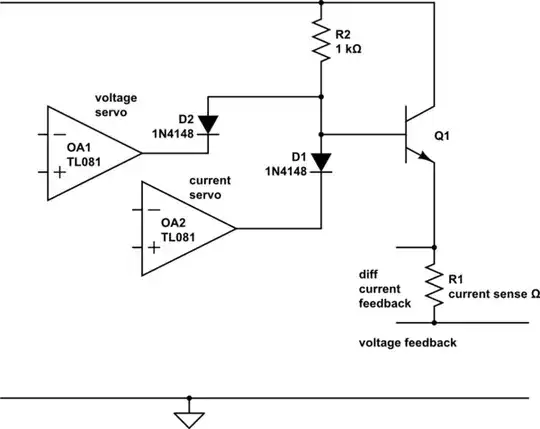
simulate this circuit – Schematic created using CircuitLab
Here is my problem, I need to design a fairly accurate programmable constant voltage and constant current circuit (the output needs to be 0.1% and within 100uV of the DAC input) the constant current portion also needs a similar accuracy and to be able to source 200mA at 0V to 7V.
I also have temperature req's and noise req so I'll be building this with low tempco opamps low noise op amps. I'm not so worried about that now. Right now I'm trying to find a good circuit topology, which in all the literature that I have this type of circuit is not covered. I don't want to use a DC to DC because of the ripple.
What is a circuit topology that I can use to build a precision CC/CV circuit?
(I could also use a precision LDO if needed) Bonus points if it can source and sink current, I can build the rails around the circuit.