so i'm trying to design a CPU and in all my previous designs i have used a cascade adder but i want to try using a fast adder to speed things up. when i search for "8 bit fast adders" all i get is the 4 bit fast adder designs and i don't want to link all the carry ins and outs together so does anyone have a true 8 bit fast adder design. all i want is the diagram, which means only the logic gates(and gate, or gate, etc) no blocks or anything like that. for an 8 bit adder with fast carry no other operations just adding.
-
there are multiple adders implementations in the dedicated [Wiki](https://en.wikipedia.org/wiki/Adder_(electronics)) page. Pick the one you like. – Eugene Sh. Mar 29 '17 at 16:00
-
that's a pretty cool project, but maybe you'd want to look into how automated design tools implement single-cycle adder. I've had some kind of a look at single-cycle multipliers in my answer [here](https://electronics.stackexchange.com/questions/280673/why-does-hardware-division-take-much-longer-than-multiplication/280695#280695). You probably don't want exactly that architecture (which is FPGA-specific) in your CPU, but really, the complexity of a "fast multiplier" is staggering, and I don't believe you "need" to implement an adder on your own if you'd use any common RTL to describe your CPU. – Marcus Müller Mar 29 '17 at 18:46
1 Answers
The question what makes an adder "fast" is often a technological one – are you implementing (or simulating it) for ASIC, or some specific FPGA?
In either case, you'll have elementary "building blocks" that you'll "plug together"; it's really not like your usually dealing with "AND" and "OR" components when describing a CPU design.
As an example, take this minimal 8-bit adder Verilog module:
module add (clk, a, b, result);
   input clk;
   input [7:0]a;
   input [7:0]b;
   output [15:0]result;
   always @(posedge clk)
     result = a + b;
endmodule // add
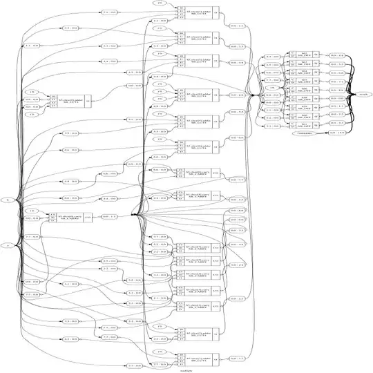
Implemented for an ICE40 FPGA, it would look like this. Notice that the blocks here are the elementary building blocks. There's no AND/OR here – so optimizing an adder for speed with those makes zero sense:
compare that to the more abstract "general" techmap that yosys (which I'm using to generate these trees) generates:
You'll see your AND, XOR, XNOR, NAND "gate" primitives in there, but also things like AOI (and-or-invert) – which the software deems useful, because they might map to something specifically easy and compact to implement on any given architecture, be it an FPGA or ASIC cells.
So, generally, it is important to understand what logic constitutes a complex operation such as "add". However, as soon as your optimizing that for speed, size, power, you'll have to consider the actual thing that will implement that – be it an ASIC, be it something built from 74xx or be it an FPGA – and a general rule like "this is a fast implementation" cease to exist.
- 105
- 1
- 1
- 6
- 88,280
- 5
- 131
- 237
-
I actually was looking for more of a non fpga approach so thankyou marcus müller but what would the circuit diagram of the oai or aio or any of those that are in there – keco2002 Mar 30 '17 at 20:14
-
1@keco2002 you're missing my point: that depends on what elements you can have in your circuit. In my circuits, I can have AIOs. – Marcus Müller Mar 30 '17 at 23:17
-
Ah i see, so everyone has ther own sort of design for a fast adder depending on the application? – keco2002 Apr 01 '17 at 03:21
-
Exactly, and very much depending on the technology they use, too! – Marcus Müller Apr 01 '17 at 07:16
-
...and the technology vendor knows more about what works well in their technology than you do... – Chris Stratton Oct 19 '17 at 20:55

