11

I'm laying out a very space constrained PCB. Normally I would place a 25MHz crystal absolutely as close as possible to the chip using it. However, on this PCB, something else really needs the space that the crystal would be.

How bad is it really to move the crystal about 5-7mm from the chip?

Rough sketch of 25MHz crystal layout

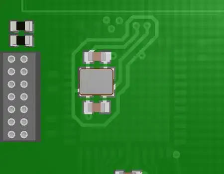
The PCB is mostly digital electronics, but there will be some analog stuff about 20mm from the crystal.

Rocketmagnet
  • 26,933
  • 17
  • 92
  • 177

1 Answers1

11

7 mm between a 25 MHz crystal and the chip driving it is no big deal. What is far more important is that the ground side of the crystal caps connect back to a ground pin on the part, not just punched thru to the ground plane. You don't want those high frequency currents running accross the ground plane else it will become a center-fed patch antenna. All the ground pins and other immediate ground connections to the chip (like the crystal caps) should be connected in a net with lines as short as you can manage, then that net connected to the main ground in one place only. This keeps all the little high frequency currents local, with only the external currents flowing accross the ground plane.

Olin Lathrop
  • 310,974
  • 36
  • 428
  • 915
  • So, one should star connect those ground pins that carry high frequency to the main ground in one place, right? Or is it not appropriate to call it star connection? I guess this technique is the one in [this answer](http://goo.gl/Ew7Jz) of yours. If possible, can you demonstrate that technique, please? – abdullah kahraman Mar 30 '12 at 09:29
  • @abdullah: This would be a perfect thing to write a paper on here, but the system isn't set up for that. See the meta question http://meta.electronics.stackexchange.com/q/1051/4512. I've also learned my lesson from http://electronics.stackexchange.com/q/28251/4512 about trying to do with with a question. I spent a lot of time and it essentially got taken away from me. No thanks. – Olin Lathrop Mar 30 '12 at 12:30
  • Why don't you just create a paper and put it on your website? I think it would be great that you created your own blog, shared your knowledge. – abdullah kahraman Mar 30 '12 at 12:37
  • @abdullah: I might do that and have occasionally done it in the past, but few people would know to look for it. What this site could offer, if done right, is to bring a lot of eyeballs to the paper, thereby making it worthwhile to write. – Olin Lathrop Mar 30 '12 at 13:08
  • 1
    If you create a separate blog, using something like [WordPress](http://wordpress.org/), and link in your profile, most of the guys here will be your regular subscribers -including me. – abdullah kahraman Mar 30 '12 at 13:10
  • @OlinLathrop: What if I punched the via through to the QFN's thermal pad, but made sure it didn't connect to the GND plane? – Rocketmagnet Apr 08 '12 at 14:25
  • @Rocket: The important thing is that the ground side of the caps have a short path to the chip ground. Check the datasheet whether the thermal pad is meant to handle ground current, or is just supposed to be connected to ground. Generally you'd connect the thermal pad on the circuit board directly to all the ground pins of the chip, assuming the thermal pad is supposed to be connected to ground. If so, what you are suggesting would be fine. – Olin Lathrop Apr 08 '12 at 14:51