21

I am designing a very dense PCB containing a 0.4mm pitch QFN chip. In parts it is proving very difficult to fan out. It is made all the more difficult by the huge thermal pad that all QFNs have for some reason.

It is reasonable to place tiny vias 0.45mm OD, 0.2mm ID between the land pads and the thermal pad, like this? enter image description here

I can't think of a good reason why not: they're covered in solder resist, and the sizes and clearances are within spec for our PCB shop. But I don't think I've ever seen anyone do this before.

Add

I just wanted to add some photos for people interested in these small vias. Here's two from a board we had made recently. Some of the drills are bang on, and some are slightly off.0.2mm via holes

Rocketmagnet
  • 26,933
  • 17
  • 92
  • 177

2 Answers2

13

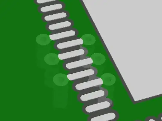
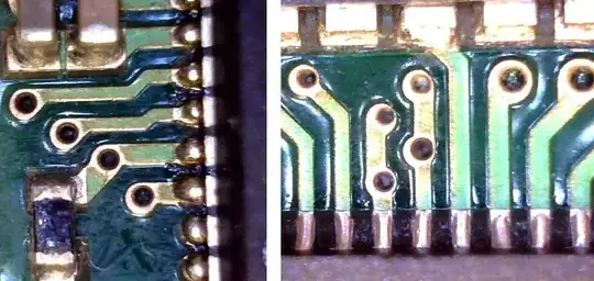
If those clearances are in spec for your shop, you're using a very advanced shop. The drill registration, in particular, must be very good.

Normally, the pad around the via is just big enough so that if the drill hole is off center (to the limits of its tolerance), the hole won't break out more than x % of the perimeter of the pad.

If that's what you're doing here, I suspect you have a potential problem. If the drill hole goes off toward the QFN pad enough to break out of the via pad, it will not have any solder mask between it and the QFN pad. Then, when you lay down solder paste and reflow the QFN part, its possible for all the solder to get sucked down the via, leaving you with no connection (or a very dodgy connection) to the QFN part.

If your via pads are actually much oversized so that there's no risk of the via hole being outside the solder-mask area, then you could be okay. But that's probably still requiring very tight drill tolerance. If this is a one-off, no problem. If you want to take this to production, first make sure your production shop can meet the same tolerances at a price you're willing to pay for this board.

An alternative might be to do "via-in-pad, plated-over" (VIPPO). That puts the via right in the pad, then deliberately fills it with solder or some kind of polymer so it won't suck solder away from the joint with the part. But I'm not sure if you can do that with a very small pad like you've drawn here.

The Photon
  • 126,425
  • 3
  • 159
  • 304
  • 2
    I agree it's an amazingly tight tolerance, but they seem to offer it as standard. I've had boards manufactured with these vias before, and they seem to have come out alright. – Rocketmagnet Mar 27 '12 at 22:47
  • Good point about the drill tolerance though. If I move the via by 0.05mm, I can get it far enough from the pad that this won't happen, and it's still inside the solder mask on the thermal pad side. – Rocketmagnet Mar 27 '12 at 22:48
  • 2
    Another trick that I use is to stagger vias on the outside. You can make the drills a bit larger too. Basically the first pin has a via going away from the IC the distance you have it now. The next pin goes out a few mils further before it goes to the via. the third pin matches the first, so on. This might not work in your situation, I didn't feel like going through the math for this comment. – Kris Bahnsen Mar 27 '12 at 22:54
  • @Rocketmagnet: That's basically 8/18 vias. I used that on a recent board at great expense. What's the manufacturer? – darron Mar 27 '12 at 23:29
  • 2
    http://www.pcbtrain.co.uk/schematic/pcb-train-technical-capability/ – Rocketmagnet Mar 28 '12 at 07:31
  • @Kris: Yes, I do that usually, but in this case, there isn't really room for that either. Problem is that a track can't actually squeeze between two vias, so the vias have to be moved apart a little, which starts to encroach on the space for the decoupling cap. – Rocketmagnet Mar 28 '12 at 09:24
  • Can you reduce the trace width a little bit when going between the caps? I've seen this termed "necking down" before. I suppose it's impossible if you're already at the trace width limit for your manufacturer, though – ajs410 Jun 06 '12 at 22:00
  • @ajs410, yes, the limitation is the space/trace rules of your vendor, as well as the clearance you'll need from the capacitor's pad to avoid solder bridging with worst-case solder mask alignment (another rule that depends on the capabilities of your vendor). – The Photon Jun 06 '12 at 22:51
11

There are some awful QFN packages (DQFN) with two rows of pads where you absolutely have to do this, so I can confirm that it is possible. @The Photon covered all of the dangers of doing this better than I could.

This application note has some good general guidelines.

For reference, here's a picture the DQFN-124 that I'm working with right now:
enter image description here
The only saving grace of DQFN is that the thermal pad is much smaller, so you have a bit of breathing room for the vias. The signal vias in the picture are a 10 mil drill with 8 mil traces -- any larger and it becomes very difficult to escape all of the pins. Dedicated ground and power planes (not shown, 4-layer board) are almost mandatory as well.

Joe Baker
  • 1,713
  • 1
  • 16
  • 30
  • 2
    I moved the image in your post to an inline image (it's interesting!), and moved the link to the app note. – Connor Wolf Jun 06 '12 at 04:25
  • 1
    Huh. If they can make the thermal pad smaller for DQFNs, why can't they do it for QFNs? – Rocketmagnet Jun 06 '12 at 09:06
  • 1
    my god, whose part is that? – akohlsmith Jun 07 '12 at 02:38
  • Agree with @AndrewKohlsmith. It's kind of an interesting footprint...I have done one similar to that but the spacing of the inside pads was offset from the outer ones, so you could at least route to the inner pads easily. I wonder why you couldn't do something like that with this package. – dext0rb Jun 07 '12 at 06:36
  • 2
    @AndrewKohlsmith It's a dual core [XMOS processor.](http://www.xmos.com/products/silicon/xs1-l2) If I had to describe it in one sentence, I would go with "a microcontroller and an FPGA had a baby". It's a really neat piece of hardware, but I'll be a much happier camper later this year when they release the next generation's dual core variant in a proper BGA package. – Joe Baker Jun 07 '12 at 07:09
  • @Rocketmagnet I would imagine they can, but the bigger thermal pad will transfer heat more efficiently. It's a design tradeoff for a normal QFN, but you don't really have a choice with DQFN. – Joe Baker Jun 07 '12 at 07:18
  • 2
    @JoeBaker - I'm sure that most devices in QFN packages don't need the thermal pad to be *that* big, as evidenced by the fact that when they're in TQFP packages, they can get away with *no thermal pad* at all. – Rocketmagnet Jun 07 '12 at 08:10
  • @JoeBaker ahh yes, I've heard of (and read the datasheet for) XMOS before. – akohlsmith Jun 07 '12 at 11:24
  • 1
    @Rocketmagnet if you'll look at the thermal dissipation for TQFP devices, they are usually nowhere NEAR as good as QFN with large pads. If you don't need to draw so much current, or have an environment where you can push a lot of air across it the TQFP is sufficient, but if you really need to get the heat out, you'll get the QFN package variant. – akohlsmith Jun 07 '12 at 11:25
  • 1
    @AndrewKohlsmith - The other reason to get the QFN package is size. If you really need the space, but don't have large power dissipation, then you get punished with a totally unneeded thermal pad. – Rocketmagnet Jun 07 '12 at 12:31
  • @JoeBaker - +1 just for the "a microcontroller and an FPGA had a baby" line. – Connor Wolf Jan 21 '13 at 02:11