328

There are a lot of poorly drawn schematics here. A few times people have actually asked for critiques of their schematics. This question is intended as a single repository on schematic drawing rules and guidelines can point people to. The question is

What are the rules and guidelines for drawing good schematics?

Note: This is about schematics themselves, not about the circuits they represent.

Olin Lathrop
  • 310,974
  • 36
  • 428
  • 915

8 Answers8

435

A schematic is a visual representation of a circuit. As such, its purpose is to communicate a circuit to someone else. A schematic in a special computer program for that purpose is also a machine-readable description of the circuit. This use is easy to judge in absolute terms. Either the proper formal rules for describing the circuit are followed and the circuit is correctly defined or it isn't. Since there are hard rules for that and the result can be judged by machine, this isn't the point of the discussion here. This discussion is about rules, guidelines, and suggestions for good schematics for the first purpose, which is to communicate a circuit to a human. Good and bad will be judged here in that context.

Since a schematic is to communicate information, a good schematic does this quickly, clearly, and with a low chance of misunderstanding. It is necessary but far from sufficient for a schematic to be correct. If a schematic is likely to mislead a human observer, it is a bad schematic whether you can eventually show that after due deciphering it was in fact correct. The point is clarity. A technically correct but obfuscated schematic is still a bad schematic.

Some people have their own silly-ass opinions, but here are the rules (actually, you'll probably notice broad agreement between experienced people on most of the important points):

  1. Use component designators

    This is pretty much automatic with any schematic capture program, but we still often see schematics here without them. If you draw your schematic on a napkin and then scan it, make sure to add component designators. These make the circuit much easier to talk about. I have skipped over questions when schematics didn't have component designators because I didn't feel like bothering with the second 10 kΩ resistor from the left by the top pushbutton. It's a lot easier to say R1, R5, Q7, etc.

  2. Clean up text placement

    Schematic programs generally plunk down part names and values based on a generic part definition. This means they often end up in inconvenient places in the schematic when other parts are placed nearby. Fix it. That's part of the job of drawing a schematic. Some schematic capture programs make this easier than others. In Eagle for example, unfortunately, there can only be one symbol for a part. Some parts are commonly placed in different orientations, horizontal and vertical in the case of resistors for example. Diodes can be placed in at least 4 orientations since they have direction too. The placement of text around a part, like the component designator and value, probably won't work in other orientations than it was originally drawn in. If you rotate a stock part, move the text around afterward so that it is easily readable, clearly belongs to that part, and doesn't collide with other parts of the drawing. Vertical text looks stupid and makes the schematic hard to read.

    I make separate redundant parts in Eagle that differ only in the symbol orientation and therefore the text placement. That's more work upfront but makes it easier when drawing a schematic. However, it doesn't matter how you achieve a neat and clear end result, only that you do. There is no excuse. Sometimes we hear whines like " But CircuitBarf 0.1 doesn't let me do that". So get something that does. Besides, CircuitBarf 0.1 probably does let you do it, just that you were too lazy to read the manual to learn how and too sloppy to care. Draw it (neatly!) on paper and scan it if you have to. Again, there is no excuse.

    For example, here are some parts at different orientations. Note how the text is in different places relative to parts to make things neat and clear.

    Don't let this happen to you:

    Yes, this is actually a small snippet of what someone dumped on us here.

  3. Basic layout and flow

    In general, it is good to put higher voltages towards the top, lower voltages towards the bottom and logical flow left to right. That's clearly not possible all the time, but at least a generally higher level effort to do this will greatly illuminate the circuit to those reading your schematic.

    One notable exception to this is feedback signals. By their very nature, they feed "back" from downstream to upstream, so they should be shown sending information opposite of the main flow.

    Power connections should go up to positive voltages and down to negative voltages. Don't do this:

    There wasn't room to show the line going down to ground because other stuff was already there. Move it. You made the mess, you can unmake it. There is always a way.

    Following these rules causes common subcircuits to be drawn similarly most of the time. Once you get more experience looking at schematics, these will pop out at you and you will appreciate this. If stuff is drawn every which way, then these common circuits will look visually different every time and it will take others longer to understand your schematic. What's this mess, for example?

    After some deciphering, you realize "Oh, it's a common emitter amplifier. Why didn't that #%&^$@#$% just draw it like one in the first place!?":

  4. Draw pins according to function

    Show pins of ICs in a position relevant to their function, NOT HOW THEY HAPPEN TO STICK OUT OF THE CHIP. Try to put positive power pins at the top, negative power pins (usually grounds) at the bottom, inputs at left, and outputs at right. Note that this fits with the general schematic layout as described above. Of course, this isn't always reasonable and possible. General-purpose parts like microcontrollers and FPGAs have pins that can be input and output depending on use and can even vary at run time. At least you can put the dedicated power and ground pins at top and bottom, and possibly group together any closely related pins with dedicated functions, like crystal driver connections.

    ICs with pins in physical pin order are difficult to understand. Some people use the excuse that this aids in debugging, but with a little thought you can see that's not true. When you want to look at something with a scope, which question is more common "I want to look at the clock, what pin is that?" or "I want to look at pin 5, what function is that?". In some rare cases, you might want to go around a IC and look at all the pins, but the first question is by far more common.

    Physical pin order layouts obfuscate the circuit and make debugging more difficult. Don't do it.

  5. Direct connections, within reason

    Spend some time with placement reducing wire crossings and the like. The recurring theme here is clarity. Of course, drawing a direct connection line isn't always possible or reasonable. Obviously, it can't be done with multiple sheets, and a messy rats nest of wires is worse than a few carefully chosen "air wires".

    It is impossible to come up with a universal rule here, but if you constantly think of the mythical person looking over your shoulder trying to understand the circuit from the schematic you are drawing, you'll probably do alright. You should be trying to help people understand the circuit easily, not make them figure it out despite the schematic.

  6. Design for regular size paper

    The days of electrical engineers having drafting tables and being set up to work with D size drawings are long gone. Most people only have access to regular page-size printers, like for 8 1/2 x 11-inch paper here in the US. The exact size is a little different all around the world, but they are all roughly what you can easily hold in front of you or place on your desk. There is a reason this size evolved as a standard. Handling larger paper is a hassle. There isn't room on the desk, it ends up overlapping the keyboard, pushes things off your desk when you move it, etc.

    The point is to design your schematic so that individual sheets are nicely readable on a single normal page, and on the screen at about the same size. Currently, the largest common screen size is 1920 x 1080. Having to scroll a page at that resolution to see necessary detail is annoying.

    If that means using more pages, go ahead. You can flip pages back and forth with a single button press in Acrobat Reader. Flipping pages is preferable to panning a large drawing or dealing with outsized paper. I also find that one normal page at reasonable detail is a good size to show a subcircuit. Think of pages in schematics like paragraphs in a narrative. Breaking a schematic into individually labeled sections by pages can actually help readability if done right. For example, you might have a page for the power input section, the immediate microcontroller connections, the analog inputs, the H bridge drive power outputs, the ethernet interface, etc. It's actually useful to break up the schematic this way even if it had nothing to do with drawing size.

    Here is a small section of a schematic I received. This is from a screenshot displaying a single page of the schematic maximized in Acrobat Reader on a 1920 x 1200 screen.

    In this case, I was being paid in part to look at this schematic so I put up with it, although I probably used more time and therefore charged the customer more money than if the schematic had been easier to work with. If this was from someone looking for free help like on this web the site, I would have thought to myself screw this and gone on to answer someone else's question.

  7. Label key nets

    Schematic capture programs generally let you give nets nicely readable names. All nets probably have names inside the software, just that they default to some gobbledygook unless you explicitly set them.

    If a net is broken up into visually unconnected segments, then you absolutely have to let people know the two seemingly disconnected nets are really the same. Different packages have different built-in ways to show that. Use whatever works with the software you have, but in any case, give the net a name and show that name at each separately drawn segment. Think of that as the lowest common denominator or using "air wires" in a schematic. If your software supports it and you think it helps with clarity, by all means, use little "jump point" markers or whatever. Sometimes these even give you the sheet and coordinates of one or more corresponding jump points. That's all great but label any such net anyway.

    The important point is that the little name strings for these nets are derived automatically from the internal net name by the software. Never draw them manually as arbitrary text that the software doesn't understand as the net name. If separate sections of the net ever get disconnected or separately renamed by accident, the software will automatically show this since the name shown comes from the actual net name, not something you type in separately. This is a lot like a variable in a computer language. You know that multiple uses of the variable symbol refer to the same variable.

    Another good reason for net names is short comments. I sometimes name and then show the names of nets only to give a quick idea what the purpose of that net is. For example, seeing that a net is called "5V" or "MISO" could help a lot in understanding the circuit. Many short nets don't need a name or clarification, and adding names would hurt more due to clutter than they would illuminate. Again, the whole point is clarity. Show a meaningful net name when it helps in understanding the circuit, and don't when it would be more distracting than useful.

  8. Keep names reasonably short

    Just because your software lets you enter 32 or 64 character net names, doesn't mean you should. Again, the point is about clarity. No names is no information, but lots of long names are clutter, which then decreases clarity. Somewhere in between is a good tradeoff. Don't get silly and write "8 MHz clock to my PIC", when simply "CLOCK", "CLK", or "8MHZ" would convey the same information.

    See this ANSI/IEEE standard for recommended pin name abbreviations.

  9. Upper case symbol names

    Use all caps for net names and pin names. Pin names are almost always shown upper case in datasheets and schematics. Various schematic programs, Eagle included, don't even allow for lower case names. One advantage of this, which is also helped when the names aren't too long, is that they stick out in the regular text. If you do write real comments in the schematic, always write them in mixed case but make sure to upper case symbol names to make it clear they are symbol names and not part of your narrative. For example, "The input signal TEST1 goes high to turn on Q1, which resets the processor by driving MCLR low.". In this case, it is obvious that TEST1, Q1, and MCLR refer to names in the schematic and aren't part of the words you are using in the description.

  10. Show decoupling caps by the part

    Decoupling caps must be physically close to the part they are decoupling due to their purpose and basic physics. Show them that way. Sometimes I've seen schematics with a bunch of decoupling caps off in a corner. Of course, these can be placed anywhere in the layout, but by placing them by their IC you at least show the intent of each cap. This makes it much easier to see that proper decoupling was at least thought about, more likely a mistake is caught in a design review, and more likely the cap actually ends up where intended when the layout is done.

  11. Dots connect, crosses don't

    Draw a dot at every junction. That's the convention. Don't be lazy. Any competent software will enforce this any way, but surprisingly we still see schematics without junction dots here occasionally. It's a rule. We don't care whether you think it's silly or not. That's how it's done.

    Sort of related, try to keep junctions to Ts, not 4-way crosses. This isn't as hard a rule, but stuff happens. With two lines crossing, one vertical the other horizontal, the only way to know whether they are connected is whether the little junction dot is present. In past days when schematics were routinely photocopied or otherwise optically reproduced, junction dots could disappear after a few generations, or could sometimes even appear at crosses when they weren't there originally. This is less important now that schematics are generally in a computer, but it's not a bad idea to be extra careful. The way to do that is to never have a 4-way junction.

    If two lines cross, then they are never connected, even if after some reproduction or compression artifacts it looks like there maybe is a dot there. Ideally connections or crossovers would be unambiguous without junction dots, but in reality, you want as little chance of misunderstanding as possible. Make all junctions Ts with dots, and all crossing lines are therefore different nets without dots.

Look back and you can see the point of all these rules is to make it as easy as possible for someone else to understand the circuit from the schematic, and to maximize the chance that understanding is correct.

  • Good schematics show you the circuit. Bad schematics make you decipher them.

There is another human point to this too. A sloppy schematic shows lack of attention to detail and is irritating and insulting to anyone you ask to look at it. Think about it. It says to others "Your aggravation with this schematic isn't worth my time to clean it up" which is basically saying "I'm more important than you are". That's not a smart thing to say in many cases, like when you are asking for free help here, showing your schematic to a customer, teacher, etc.

Neatness and presentation count. A lot. You are judged by your presentation quality every time you present something, whether you think that's how it should be or not. In most cases, people won't bother to tell you either. They'll just go on to answer a different question, not look for some good points that might make the grade one notch higher, or hire someone else, etc. When you give someone a sloppy schematic (or any other sloppy work from you), the first thing they're going to think is "What a jerk". Everything else they think of you and your work will be colored by that initial impression. Don't be that loser.

TeilZeitGott
  • 149
  • 9
Olin Lathrop
  • 310,974
  • 36
  • 428
  • 915
  • +1 I realy like it. But one question: In one of your answers you complained about a schematic, that was colored. Would you say, that it is good practice to always make the schematic monochrome? Link to the mentioned answer: http://electronics.stackexchange.com/a/26487/4950 – PetPaulsen Mar 17 '12 at 20:26
  • 27
    My ten cents: though I love to use colour to disambiguate on-screen, I prefer the way monochrome schematics look *in print* (or PDF). Conventions and æsthetics evolved for monochrome work, and not everyone has access to a colour printer/photocopier so colour information may be lost. I also like to not **depend** on colour (one of my co-workers is colour-blind, which occasionally leads to semi-amusing incidents involving colour-coded LED status lights. So I've become very sensitive to this). – Alexios Mar 17 '12 at 21:21
  • Well done. +1 I find it interesting that my school lacks a course on proper circuit drafting. It should be a required course for freshman. I guess they just assume people will catch on. – atomSmasher Mar 18 '12 at 05:18
  • 3
    As in programming, readability counts. From the Zen of Python: "Beautiful is better than ugly." – shimofuri Mar 18 '12 at 11:07
  • 25
    Maybe it's because of my programming background, but I find that I often prefer "air wires" for many things. If I see two pins on the CPU labeled "DATA_TO_FTDI" and "DATA_FROM_FTDI", I can tell at a glance that those pins go to (or at least should) the data RX/TX pins on the FTDI chip. A glance at the FTDI chip can confirm that. I can then check those names against the definitions of the pins on the device (since some devices which behave as communication bridges use TX as an output (they transmit data on that pin), while others use it as an input (accepting data to be transmitted elsewhere). – supercat Mar 21 '12 at 17:20
  • 19
    @supercat - The issue with air-wires is that even if where they go seems apparent, you can never be sure (without an exhaustive search), that you have found *everywhere* they go. For your "DATA_TO_FTDI" example, what if there is a serial activity LED on that bus? Or another device sharing the serial interface? I can never be sure without manually looking over **EVERY** net-label on the entire schematic. – Connor Wolf Mar 21 '12 at 21:22
  • 7
    While air-wires may work ok on simple projects, as soon as you have more then a few ICs, or your schematic grows to more then one page, it completely falls apart. Also, it's absolute poison in any environment where you have multiple people working with the schematics. The analogy between air-wires and GOTO is very apt. They both let you make short-cuts, and both make the resultant system FAR harder to maintain. – Connor Wolf Mar 21 '12 at 21:25
  • 4
    The TIA schematics found at http://www.atariage.com/2600/archives/schematics_tia/index.html make heavy use of air wires, but I can't imagine that drawing in all the "air wired" connections would make them any clearer. Even without automated systems to find net connections, I can't imagine that drawing in all the connections to HΦ1/HΦ2, or D0-D7, or the write-address decodes from the bottom of page 2, etc. would make the schematics any clearer. Actually, I'm rather impressed with those schematics; indeed, they're better than a lot of newer ones. – supercat Mar 21 '12 at 22:12
  • 2
    @supercat - You are correct in that drawing in all the air-wires on that schematic would be confusing. That is because that schematic should be using a **bus**. It *would* be much more readable with a bus instead of half a dozen air-wires. – Connor Wolf Mar 26 '12 at 13:42
  • @FakeName: Which signals would you combine into what buses? D0-D7 could perhaps be a bus, though I'm not sure that would clarify much since it's mostly used piecemeal. There are 45 write addresses decoded on page 2, each of which is used on one other page (the reference near the write-decode circuitry notes which one); should those be buses? Incidentally, how do you like the use of boxes for repeated circuit elements? I think it aids comprehension, but I've not seen things drawn like that on any computer-assisted schematics (I've seen simulation tools with user-defined parts, but... – supercat Mar 26 '12 at 15:02
  • ...never drawn as they are on the TIA schematics). I think they make things a lot clearer than they would be if everything was simply "copied out". – supercat Mar 26 '12 at 15:03
  • In some cases of high complexity, Schematics should list in a small table, last Ref Des used,for each type. and unused Ref Des, (if deleted.) e.g. Highest REFDES: but for mult-page complex instruments, REFDES should be zoned for each functional of physical block zones. i.e. U1~99 even if there are only a few,,, then U100~.. with dotted lines for each zone and Function Label. so Physical Zones and Logical RefDes make sense. e.g. PLL U400~U412, C400~C428, R400~R433,, etc PLL is zone PCA400 with ref des for that card in same block. – Tony Stewart EE75 May 15 '12 at 05:36
  • 5
    "Why didn't that #%&^$@#$% just draw it like one in the first place!?" Ugh, yes. Every single time I get a schematic from our Chinese factories it is like this. You don't win a prize for cramming the entire schematic onto on page! – endolith May 15 '12 at 16:41
  • 1
    This is a really long answer with lots of independent points. It would be best if each point were its own answer so we could comment and vote on each individually. – endolith May 15 '12 at 16:47
  • +1 for *CircuitBarf*. Also, @Olin, this is a really great reference and answer. – JYelton Dec 11 '12 at 15:13
  • 8
    One additional rule you should consider adding: "Use the same signal names in the schematic as in the source code of your firmware". This makes the whole project easier to document and maintain, and also makes communication easier between the hw designer(s) and the sw designer(s) in case they are different people. – Lundin Aug 11 '14 at 06:32
  • 1
    I know this is already quite old and still good, but some people are more the visual kind, and maybe someone of those who know the dos and donts could add some more really good do and donts examples. For the existing ones, it is almost enough to read the heading, look at the image and know what you mean. – PlasmaHH Jan 29 '15 at 16:52
  • 1
    I'm curious how far you would go to group together like pins on a microcontroller. For instance: http://imgur.com/82K8VwQ This nicely puts the power pins at the top, the ground pins at the bottom, and groups together the dedicated crystal pins. Grouping together the IO ports like this is nice for a general-use part, but for this particular application, it could be a little tidier if the programming and SPI pins were each grouped together. But is that worth it? Especially when things like the CS pins can change from revision to revision? – Rick Yorgason Apr 03 '16 at 05:53
  • 1
    I've got into a new habit (it keeps me honest and perhaps helps the end-user realize a safe assumption) of adding small text showing logic level threshold values (Vin H/L and Vout H/L) parked next to the relevant IC's, FETs, etc. For example, in mixed logic families, a 5V ACT buffer feeding a 3.3V LVC buffer showing the V levels and that due diligent was exercised. – Steve Jul 10 '19 at 22:52
  • There is one point I don't think was mentioned in the text. An alternative to depicting lines that cross but do not join is to show it as a small bridge as in [this image, top right](https://www.dummies.com/wp-content/uploads/307565.image0.jpg) taken from "Electronics for Dummies". This may be a bit old school, but effective and may still available in some CAD packages. One other thing I was taught back in the day was to keep lines horizontal and vertical as far as possible, use diagonals sparingly. – Peter Jennings Sep 23 '19 at 09:45
38

1. Show Your Work A Schematic Diagram is intended to be the documentation of a circuit. As such, I highly recommend including any simple equations that may be used. This includes LED current calculations, filter corner frequencies, etc. Show your work, so that the next guy who has to read the schematic can check it easily.

2. Indicate UART Direction Since UART lines are not always clear which way they are flowing, add a little arrow next to each line to show the direction.

3. Be Consistent Don't use VDD in one place and 3V3 in another. Standardize.

4. Annotate Liberally This is like comments in source code. If you copied a circuit from a datasheet, put the reference on the schematic so that someone else (or you) can check it later.

19

Here's my two cents

1. Break it down Break down your design into modules. Put a block diagram of the system on the first page of the schematic

2. Answer who, what, where, when, why Who - For each module page, label "who" the module connects to. Lay it out left to right so it reads like English.

What - In the title, indicate what the module is. For instances where there are multiple I/O blocks (i.e. UART and USB), label it as such on the page.

Where - Use free text in the CAD program to indicate component placement. For example - a decoupling cap should be placed as close to the IC as possible. This will act as a quicker reference when laying out the board than referring to some other documentation.

When - Are there any timing considerations such as power supply sequencing or power fail circuitry? Put these requirements not only in a design doc but in free text on the pertinent module page.

Why and How - This belongs in an accompanying design document to verify such things as
a. Scope - what does the circuit do, what does it not do as agreed upon by the stakeholders for the project.
b. Theory of operation
c. Rationale of why the approach was taken as opposed to others. This is crucial as it serves as a history for the circuit down the road when you (or someone else) inherits/ports the design to be mindful of the same decisions as the original designer.
d. Layout considerations
e. References to other documentation.
f. Power dissipation calculations - prove not only that it works, but that calculated power dissipation for all components is some degree less than the rating for the component AND at all operational temperatures.

3. Style This is up to you and the rest of the team, but in general I prefer the following
a. Title page/block diagram
b. One "block" per page, partitioning large pin-count components (i.e. a microcontroller) into meaningful discrete symbols. This takes some time to do, but is well worth the readability.

The modularization also allows you to "tear a page out" and re-use it in other designs

c. For each component indicate the reference designator, whether or not is is a no-pop, the value/tolerance of the component, the power rating where applicable, and the package size and some way of determining the manufacturer part number. The last point will help you to make common some of the components to reduce setup manufacturing costs and to make a judgement call if some of the design parameters can be relaxed to reduce the number of different components used on the board. For vertically aligned components, place this text on the left. For horizontally aligned components, place this text above the component.

d. Lay out the circuit from left to right indicating where the module interfaces are with text

e. For power rails clarity, DO NOT USE VDD or VCC as they are ambiguous. Make a new symbol for explicitly declaring what the voltage is. Same thing for ground (i.e. GND for ground and AGND for analog ground).

Neil_UK
  • 158,152
  • 3
  • 173
  • 387
cowboydan
  • 759
  • 5
  • 9
17

R100, R101, R102 Instead of R1, R2, R3

I would like to share my experience in assigning names for components.

Identify the blocks of circuits according to the functions. Even if it is a complex circuit, you can identify them such as main power stage, pre-amplifier, amplifier, A/D conversion section, indicator/transducer blocks, synchronizing section, timer or any other logical operation sections.

My suggestion is name the components using larger numbers like R100, R101, R102 instead of R1, R2, R3... etc.

You can assign 100, 200, 300 ... etc for each block you identified. For example, you can assign 100 to 199 numbers for power section. Then all components in the power section in 1xx form such as Q100, R101, R103, C100, D100, D106.

Advantage

  • Its easy to identify the sections of a circuit by function wise in a complex schematic diagram.
  • Easy to troubleshoot.
  • Its easy to name the parts when you have to add new components to a section later. Because you have about 100 name options to select.
  • Easy to drawing PCB layouts in any cad software manually. Because at the very beginning of the PCB drawing each type of components are gathered at one place. enter image description here

You can easily separate them into different places by its number without looking many times at the schematic.

lighthouselk
  • 29
  • 1
  • 5
11

A couple of points in addition to the ones posted above. The first answer is fairly heroic but there's one thing I don't agree with.

Pin order in schematic symbol.

Why to reorder pins It makes aesthetically more pleasing schematic that may be easier to interpret depending on how the pins are laid out.

Why not to reorder pins It's asking for trouble, period. In the datasheet the pins are given as they are in the physical chip so you create a significant source of error if you start rearranging them. Not only it makes prototyping more difficult, you're also inviting errors in the physical pinout. In a design review pinouts are compared and if they're mishmash, it's easy to get mixed up.

Another comment on "air wires" Just don't do it. Instead use ports which require you to explicitly make a connection between two nets in same or separate schematic sheets. If you allow nets to connect without ports/off-pages, you open a huge can of worms as apparently unrelated nets may be shorted in layout.

Don't pack too much stuff on a page People may start complaining if you schematic is thirty pages but the alternative is having rats nest of confusing wiring between parts. Break up the schematic into logical blocks of circuits and stick them to separate pages as necessary.

Leave enough space between pins Many premade schematic symbols pack the device pins as tightly as possible. While this minimizes the area of a symbol, it also makes the circuit more difficult to read as you have connections converging from "outside" into the tightly packed pins. You should leave enough space so you can add series resistors staggered.

Reference designators You should obviously have reference designators in schematic and layout. For anything more complex these need to be ordered. There are two approaches to it.

  1. You can ask the schematic capture program to label these so each page has it's own prefix. This way it's easy to find any given part in the BOM from the schematic. And also ECO is easier to follow as you know which page the changes are for. The downside of this is that you end up with long reference designators and finding the part in the layout can be difficult.

  2. You can ask the layout program to label these. This way you will have ordered references on the PCB which makes it much easier to locate resistor R347. Preferably on a larger PCB this should be cordoned into quadrants (sextants, octants..). The downside is that it's not obvious where the part is in the schematic. You just can't win here, either schematic is easier to read or the layout is.

Barleyman
  • 3,568
  • 14
  • 25
  • 25
    I just disagree about pin order. Schematics shouldn't necessarily have anything to do with the physical layout of the chip. For example, op amps should look like op amps in a schematic. A quad op amp should look NOTHING like the chip. Also, when dealing with complicated high pin counts, the gates should be split up into functional units. – Scott Seidman Apr 19 '16 at 12:56
  • 7
    Good points, but I agree with Scott that avoiding reordering pins is nonsense. With small chips, sure, but schematics are 100% less confusing if instead of having wires criss crossing everywhere, you reorder the pins on a chip and just make sure they are labeled properly. If out of order pins on a schem is enough to confuse someone, they probably shouldn't be messing around with the board to begin with. His op amp point is also very valid. – I. Wolfe Apr 19 '16 at 13:08
  • 1
    Opamps are a special case as I'm sure you'll agree, similar to transistors etc. If you end up with a respin because your rearranging of schematic pins led into an invalid footprint, you didn't exactly do anyone favours. – Barleyman Apr 19 '16 at 13:14
  • Footprints should be compared to the data-sheet. Symbols as well. That is the only reference that counts. It makes no sense to use a self-drawn symbol as reference for the footprint. Sure there should be a consistency check between the two, but any decent software will do that and show you unconnected pins on either side. – cx05 Oct 24 '16 at 19:54
  • @cx05 Yes, which is why it makes sense to follow the datasheet representation/order with the pinout to minimize the chance of error. Obviously for a 388-pin BGA you have to break the symbols apart but still creating the symbol with the same pinout as the chip has makes it more likely you've not swapped pins. Yes, software can help if you actually can find a CAD symbol for your part. This tends to not happen with that BGA package so you're into an evening of checking and triple checking a long list of pins against your symbol. – Barleyman Oct 27 '16 at 13:19
  • Depending on your schematic capture tool you may be able to view the component pinout in schematic format where you can order it by pin number / name which allows you to break parts apart by ports etc while having an easy way to verify the pinout. For something simple like 16-pin SMPS controller when I keep the physical chip pin order I can immediately see from the schematic at a glance which pin I should be probing on the PCB. – Barleyman Oct 27 '16 at 13:22
  • Well, I prefer e.g. to have the port pins of a µC or FPGA in logical order (PA1,PA2...). Many manufacturers assign pin functions according to this ordering. This is what concerns me on a day-to-day basis. With your BGA example it would actually be impossible to mimic the pinout in the schematic. Also, pin assignment is only verified once. Many software packages will give a pin report that can be ordered in any way the user sees fit or exported and sorted in Excel. Once a component is verified, I should never need to verify the pinout again. But I guess it all comes down to use-case and taste. – cx05 Oct 28 '16 at 12:32
  • @cx05 with bga you're not going to probe anything anyways so most of the advantage is lost. For QFP et al I like to maintain the actual physical pinout, for BGAs usually whatever they use in the datasheet. – Barleyman Oct 28 '16 at 13:39
  • For me it depends, there are some parts that have conventions for how they are drawn, Opamps obviously, but also D type FF (D, Clk on the left, S/R on top/bottom Q & Q* on the right), and indeed most jellybean logic where in any case you are usually drawing a single gate and doing the pin swapping once you start the layout. Same thing with linear regulators, input on the left, ground (or reference) on the bottom and output on the right, even when the part is one with a weird pinning (7905). Obviously there are parts that do not have defined conventions and for these 1:1 is not unreasonable. – Dan Mills May 25 '17 at 12:29
  • @DanMills I don't know how many people actually do electronics for living here but getting two pins swapped is an unfortunate fact of life and anything that makes it harder to pick up in the review process makes things more painful. It's hard enough not to get cross-eyed on even something relatively minor like QFP-48, never mind large BGAs. You got a thousand parts done perfectly and the layout is rubbished plus you chalk in extra month to do a respin because you got two pins swapped. It's not like software. It's not really helpful that things like MSP430 microcontrollers mix'n'match pinouts. – Barleyman May 26 '17 at 21:50
  • My usual respin trigger is either mechanical, getting the footprint wrong on something funky (Some connectors have the worlds worst datasheets to dimension off), or a straightforward design thinko. I don't think I have ever had a respin due to swaps between designator and label in several hundred boards, that is what a shell script and the manufacturers BSDL file is for. I tell our software weanies that they will understand hardware designers when they understand that pressing compile costs ~£1,000 and takes 6 weeks to run.... – Dan Mills May 27 '17 at 00:03
  • @DanMills A thousand? Pretty cheap stuff then.. You can avoid a lot of problems with footprints if you use STEP models. I got fired actually from one job because I was "wasting time" adding step models to component symbols but those have brought out quite a few problems on mis-interpreting dimensions etc. You don't always have BDSL (or most of the time). Sometimes you get pre-made eCAD symbols which tend to be crap. Often you get nothing except datasheet with 48 pins for that PHY. I have had pins swapped and the guys looking in review specifically looking for that for that part and not get it. – Barleyman May 28 '17 at 22:55
  • Some eCAD programs let you at least copy the pinout from a datasheet assuming the manufacturer made the datasheet in a way that allows you to cut and paste them. Some do not, unless Mentor has changed PADS in recent years I had quality time with a ruler and a pencil.. – Barleyman May 28 '17 at 23:00
  • Physical pinout is just one side of the problem.. You may have bunch of functions available for each pin so a second layer of problems arises of having all the signals going to correct ports which have matching functions. With FPGAs you may be able to respec but with microcontrollers you're hosed. MSP430 is one obnoxious example with at least three different functions per pin possible. My personal favourite are LSI chips that have regular G-S-G-S style pinout except in the middle they go G-S-S-G-G-S to check if you're paying attention. – Barleyman May 28 '17 at 23:23
  • 1
    [Answer in a newer thread.](https://electronics.stackexchange.com/a/421655/7036) To your point, @ScottSeidman . – Nick Alexeev Feb 11 '19 at 17:37
  • In creating a new symbol from a datasheet, I try to import the pin list from the original doc into a spreadsheet. For OrCAD, this can be easily massaged into a form where it can be used to create a new symbol. This is MUCH less error-prone than typing in the pin list from a diagram. All bets are off though if the manufacturer locks their PDF so you can't copy-paste it. Some manufacturers will even provide you a pin list in Excel (e.g., Broadcom for their set-top-box chips) which saves a lot of time. – hacktastical Jul 11 '19 at 02:32
  • @hacktastical Yes, this is a must for large packages. I created a 176-pin BGA microcontroller part recently that would have been very difficult to do manually. It takes a bit of trial and error to find the correct dialog where you can paste pins, Altium has part pin list in several places and not all of them are editable. WRT reordering pins, it's a matter of opinion and depends. On a BGA it's out of the question since ports tend to be ordered in staggered fashion 1-4 rows deep into the package. For >100 pin packages you won't be trying to locate pins visually from schematic anyways. – Barleyman Jul 11 '19 at 12:38
  • Pin counts of over 1000, 1500, 2000 are not uncommon for big microprocessors or SoCs these days, the lion’s share of the pins being memory and power. – hacktastical Jul 11 '19 at 15:47
  • @hacktastical Depends what you work on, obviously. I mostly work on embedded devices which usually use either small-ish microcontroller (e.g. that 176-BGA Synergy µCU) or some kind of FPGA. I've worked with 488-pin packages, that's big enough for me :-p Taking the time to painstakingly copy pinouts from datasheet and hashing them in Excel definitely does reduce "oops" moments, especially if you create a processor pinout with pin functions at the same time. – Barleyman Jul 15 '19 at 13:41
5

A few more:

  • (1) Draw on normal grid.

I really hate having to deal with other people’s work that’s drawn on half-grid. It’s a huge waste of time and doesn’t add any value to the drawing.

  • (2) Use ‘physical’ style for smaller devices.

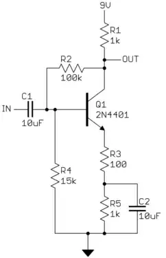
Drawing ICs and small components with the pins in order helps with conveying your intent to layout, and makes debugging much easier. This goes double for transistors and diodes in sot-23: I draw them showing the pin order, and as a result haven’t had to rework a mis-laid-out one in years.

  • (3) Realize the limits of (2) above.

It’s not possible to draw a big BGA physically, or even as one symbol. But you can at least separate by function and show how pins relate to each other spatially. For example, an FPGA can be drawn and divided to show blocks that represent logic tiles, and the tiles themselves placed / ordered on the schematic to show how they route out.

Historically, multipart symbols for elements like op-amps or gates made sense. But these are becoming more rare in designs.

  • (4) Intra-page named aliases are ok, but don’t push it.

Named aliases are the same as off-pages really: it means you still have to scan the page to look for its other instances. With a PDF schematic and Ctrl-F this isn’t as big a chore as it used to be (and shame on you manufacturers who make non-searchable PDFs. That’s just lame.) That said, off-pages are more rigorously checked by DRC than aliases.

  • (5) Block diagrams and mechanical plans are worth the effort

The effort you spend conveying your thinking here will save lots of time over the life of your design - from layout to repair. Yes, your mechanical designer will make the ‘official’ board outline, but at the very least you can convey where you expect stuff to be placed - and why - by doing these two kinds of diagrams.

  • (6) When you export your schematic to PDF, make it searchable.

Is it really too much to ask?

  • (7) Have just enough component information.

Besides the reference designator, some designers are tempted to have all the part attributes on the schematic. But do you really need them? No, you don’t. Tolerance, sometimes. Voltage, sometimes, when you have a section that’s at a higher voltage. Footprint - maybe. Manufacturer part number? Rarely - you’d want to multiple source usually. Corporate AVL/MRP number? Nope, never.

All this other stuff is what a BOM is for.

  • (7a) Think ahead to BOM generation.

That said, developing some kind of part number system even in your early days allows you to create detailed BOMs even if you don’t have an MRP system. Each part type should have a unique ID that is set as a hidden attribute in your schematic that corresponds to an entry in your master parts list (AVL list.) You use that ID later to merge in the expanded info from your AVL list to create the detailed BOM.

Even later, you can import this stuff into a real MRP or PLM system such as Oracle Agile.

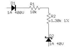
  • (8) Power is a signal, too!

It used to be that you’d draw a schematic with ‘hidden’ power / ground pins which would be automatically aliased to VCC or GND. It’s still an option when you create a symbol in Orcad for example. Don’t hide those power connections! Show ‘em! Especially considering today’s designs with multiple power domains, high power density, routing, bypassing, loop area, and so forth.

Power is so important, that if you’re not spending at least 1/3 of your time on power design you should consider another line of work.

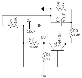
  • (9) Comments are your friend.

Highlighting key elements with text can save a lot of time in debugging. I will typically comment things that relate to software (e.g., addresses, bit locations) and power design (current typical/max, voltage).

  • (10) Size matters.

Use 11x8.5 (A size) for really simple stuff, 17x11 (B size) for most other things. Go larger only if you really need to.

17x11 (or its nearest metric equivalent) is a reasonable size for viewing on an HD screen or for printing even at 11x8.5. It’s a good go-to size to work with.

On the other hand I find that I can’t get enough stuff on 11x8.5. And on the other, other hand is the other extreme when I’ve used 23.5 x 15.2 (scaled-up B, not C) for a really complex drawing that groups together (e.g., DRAM banks): this needs to be printed at 17x11 to be reasonably easy to read in hard copy.

As it is I rarely print anything anymore, so worrying about how hard copy comes out is more trouble than it’s worth most of the time.

  • (11) Left-right signal flow, top-to-bottom power flow. Mostly.

This is the general standard to make understanding the relationships of elements easier. But sometimes giving more more weight to architecture flow than this old rule yields a clearer schematic.

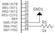
  • (12) Organize off-pages / ports in vertical groups.

It’s not necessary or useful to drag ports to the edges of the schematic. But at least line them up in organized columns so that they’re easy to scan visually.

hacktastical
  • 49,832
  • 2
  • 47
  • 138
3

The biggest dispute I see in the discussion is about pin order, but this is only a question about the bigger topics: Functional vs physical! If I make a good schematic to prepare my layout work, then it is far better to make the schematic looking as close as possible to the layout, e.g. draw the pin order not according to what someone else does in the datasheet, but as it really is. Also consider to leave a bit more space around big elements, like power devices, e.g. also draw a heatsink "symbol". If ground should be anyway a large plane, then also better go for connections by name, which also helps to avoid having many crossings. On the other hand if nobody can avoid a crossing of sensitive lines, then draw the schematic so that is becomes a guidance for good layout, e.g. the high-impedance side of a resistor divider should have usually a short connection, whereas the driving wires can be often longer without problems.
For digital IC's I tend to use automatic routers and sticking to functional order. Another controverse topic could be how to draw a differential amplifier, and e.g. a multistage amplifier, like should we draw each stage in the usual way and then wire to next stage (which often ends up in many crossings), or should we really draw the diff pairs in a symmetrical way (often done in old Tectronics osci schematics)? Here it depends also on the purpose, and how critical keeping symmetry really is. In RF circuits, having often not so many elements, I prefer again drawings very close to layout.

user32038
  • 131
  • 1
2

The schematic is a symbolic description of the function of an electronic circuit, while a layout diagram is a physical diagram clearly describing the location of components and nodes of the circuit. Schematics serve analysis, Layout displays function and assembly. A symbolic electrical diagram and a mechanical drawing, if you will. If you can clearly see the goals for those purposes, and where the overlap is, guidelines are much easier.

If I can't quickly and easily abstract the critical circuit information from the schematic, the design will be more buggy, less reliable, and more difficult to troubleshoot. If the layout doesn't show critical mechanical parameters, particularly where those impact circuit function, that drawing will be much less useful.

Where possible:

  1. Clearly decompose the function of the assembly into blocks and interfaces.
  2. Remember that power, power distribution, and decoupling are functions.
  3. Place components into blocks that are organized for analysis and completion.
  4. Signal flow left to right, power supply top to bottom, on each sheet.
  5. Interfaces on board are air connections at the edge of each sheet. Lord on the top/left, peon on the lower/right.
  6. Enumerate the sink connections on the source of each air connector.
  7. Notes, including default tolerance should appear on every page. Notes should clearly identify specific reference designators on schematic.
  8. Minimize crossing signal lines.
  9. Group related signals.
  10. Maintain order among enumerated lines. Overlap
  11. Blocks on the schematic should be located close on the assembly.
  12. Decoupling caps on the schematic should be close to the component they protect in the layout.
  13. Interface signals should be routed together.
  14. Connector pins should be numbered per the datasheet, and laid out to match the physical position of the physical connector, viewed from the top of the board.
sasguy
  • 69
  • 2