12

I'm developing a four layer board which is powered by 3 voltages - 1.8V, 3.3V and 5.0V. The board has the following stackup:

  1. Signals
  2. Ground
  3. 3.3V
  4. Signals

The ground and 3.3V plane are completely unbroken. No signal or power trace travels on them.

I'm using three LP38690DT LDOs to provide power - here's my circuit.

Power Regulators

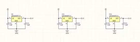
Click here for larger picture.

My concern is the layout for these devices. The datasheet suggests the following

The best way to do this is to lay out CIN and COUT near the device with short traces to the VIN, VOUT, and ground pins. The regulator ground pin should be connected to the external circuit >ground so that the regulator and its capacitors have a "single point ground".

I was somewhat confused by the term "single point ground" but I tried to follow the advice given in the datasheet to the best of my ability - but I am not sure if I am correct:

enter image description here

Note that the text in red is only there to give clarity to the folks here - I will delete it afterwards. Each regulator is connected directly to the capacitors and the ground pin of the regulator is connected directly to the capacitor's ground pin directly. Is this what the datasheet meant I should do?

The datasheet goes on to say

Since high current flows through the traces going into VIN and coming from VOUT, Kelvin connect the capacitor leads to >these pins so there is no voltage drop in series with the input and output capacitors.

What does it mean by Kelvin connect? I know what a Kelvin Connection is - what I don't understand is what does it mean in context for a LDO.

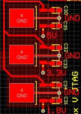
My third question is regarding all three regulators. As I mentioned, each IC is referencing ground from the same via that connects it's capacitors to the ground plane. However, should I connect all three regulators to the same ground point i.e. should all 3 regulators connect to the "single ground point/via"?

Finally, the input voltage is being fed by a 4-point through hole connector which carries 6V on two conductors and GND on the other two. The GND pins are connected direcly to the ground plane. Is this OK or should I connect the GND pins to the GND pins of the regulators directly via thick traces?

NOTE: the layout picture does not show anything connected to the output of the regulators. This is OK. I still have to connect my ICs to the power. ALSO: the maroon color underneath the regulators is not a net. This is Altium's way to show "Rooms" in PCB layout.

CURRENT REQUIREMENTS

Most of the current is drawn from the 5V supply. The 5V supply connects to a LCD display which will draw a max. of 400mA (when backlight is on) - but normally around 250mA.

The 3.3V supply will draw a max. of 300mA (discontinuous) but normally around 150mA or less.

The 1.8V is the supply for the core of the CPLDs that my board has. I was unable to estimate this but I've measured it. At startup, this was around 30mA but then reduced to 0mA. My meter, it seems, was not sensitive enough to actually measure the current. I reckon 200mA would be a safe bet for this.


UPDATED LAYOUT:

enter image description here

I hope this is what folks here meant. I wasn't sure if I should one large copper pour or three separate ones so I went with 3 separate ones.

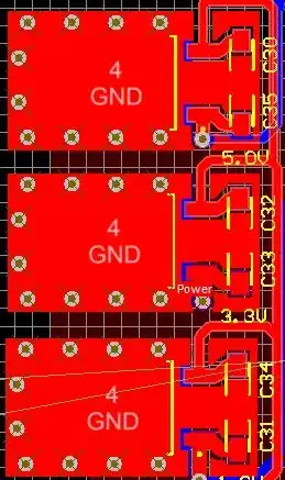
UPDATED LAYOUT (again):

enter image description here

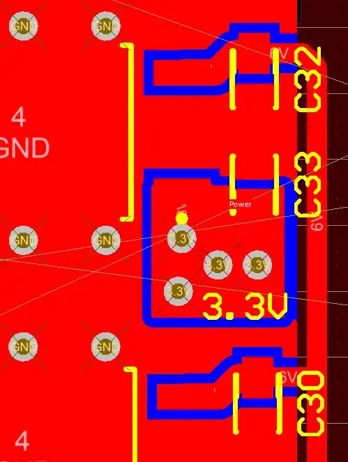
I've now made made one giant copper pour instead of 3 independent ones. I was't sure how to connect my 3.3V voltage to my power plane using multiple vias so the above is my attempt. I made a small fill and connected it directly to my output capacitor. From there I have 4 vias, each 25 mill in size, connecting directly to my power plane. Is this a better way to do it?

The clearance between the fills and other objects is about 15 mills. Should I increase this?

Saad
  • 5,319
  • 12
  • 60
  • 93
  • 2
    How much current is needed from each of these supplies? If you're approaching the 1 A limit, you may want to have multiple vias from the LDO vout to the power plane, and from the ground plane back to the LDO GND pad. – The Photon Mar 15 '12 at 16:12
  • 1
    @Saad I added some stuff to my answer based on the new info you added to your question. –  Mar 20 '12 at 22:34

4 Answers4

9

But overall you are over-thinking the importance of the GND. It's important, don't get me wrong. It's just that there are other things that are as important, and getting the GND correct is relatively easy.

You specified the voltages, you didn't specify the current. Without knowing the current, we don't know the heat generated by the LDO's. And the heat will greatly influence the way the PCB is laid out. I am going to assume that the heat generated is non-trivial.

Here's what I would do...

  1. Rotate the caps 90 degrees (sometimes clockwise, sometimes counter-clockwise). What you are doing is putting the caps GND pins together and shortening the distance between the LDO's GND and the caps.
  2. Make all of your traces wider. At least as wide as the pad it's connecting to. Use multiple VIA's if you can.
  3. Put the +6v traces "somewhere else". Either on the back side of the PCB or on the right of the LDO's. This will make sense shortly.
  4. Put a copper plane on the top layer, under and around the whole thing. Connect this to the GND layer using multiple VIAs. I would use about 10 vias per LDO, mostly around the huge GND pin. The GND pin of both the LDO's and caps should be connected to this plane DIRECTLY, without any "thermal relief". This plane should be reasonably large, although the exact size depends on the space available and how much heat the LDO's will be giving off. 1 or 2 square inches per LDO is a good start.

There are two reasons for the copper plane. 1. It gives the heat from the LDO's someplace to go to be dissipated. 2. It provides a low impedance path between the caps and the LDO.

The reason for all of the vias are: 1. It allows some of the heat to be transferred to the GND layer. 2. It provides a low-impedance path from the LDO to the GND layer.

And the reason for the fatter traces and multiple vias is simply for a lower impedance path.

I will warn you, however: Doing this will make hand-soldering of the LDO's difficult. The copper planes + vias will want to suck the heat away from the soldering iron and the solder won't stay melted for very long (if at all). You can get around this somewhat by using a hotter soldering iron, or better yet pre-heat things by using a heat gun to warm up the entire PCB first. Don't get it hot enough to melt solder (use your normal iron for that). By preheating the whole board the demands placed on your iron will be less. IMHO, this isn't a big deal but it is something to be aware of and plan for.

This method will also give you a nice connection to GND, way better than anything you've told us from the datasheets.

Update, based on new information from the original poster:

Your 5v regulator is dropping 6v to 5v (a 1 volt drop) at 400 mA. This is going to produce 0.4 watts of heat. 6v to 3.3v at 150 mA = 0.4 watts. 6v to 1.8v at 200 mA = 0.84 watts. Total 1.64 watts for all three LDO's. While this isn't crazy, it is a fair amount of heat. Meaning that you must pay attention to how this is going to get cooled otherwise it will overheat. You're well on your way to getting that done properly.

You want a single plane, not three. And the plane should extend out as far as possible, I recommend at least double the area of the LDO's themselves. The larger the plane, the better the cooling effect. If the plane is really large then you'll want to put at least four vias for every square inch. By sharing the plane, the three regulators are sharing the cooling. If you didn't do this then one regulator could get really hot while the other two are just warm.

Another optimization that you can do is with how the +6v comes in to each LDO. At the moment it goes around the cap, to the LDO. Just have it go straight into the cap, without wrapping around. This will allow you to use thicker traces and keep things a little shorter. That small amount of GND plane that wraps around the cap isn't helping much anyway.

You'll want several vias from the output of the LDO to wherever that power is going. Not just the single via that you have now.

  • 1
    David, won't this violate the "single point ground" advice given by the datasheet? If I have a plane, I no longer have a point ground where every cap and LDO ground is connected. The datasheet suggests that there have been instability cases when the single point ground was not provided and instead the caps and LDO were connected to the ground plane using separate vias. – Saad Mar 21 '12 at 10:00
  • 3
    @Saad For starters, app notes (in datasheets or by themselves) are not gospel. They frequently have errors, and this is certainly one of them. What you always want is a big fat trace between the LDO GND and the cap GND. You can't get any bigger or fatter than a plane. Next, you want a good solid connection from the LDO GND to the GND layer on the PCB. Again, you can't get any better than a bunch of VIAs. Also consider that we're talking distances of about 0.25-0.5 inches, which is very close to a "single point" anyway. –  Mar 21 '12 at 14:01
4

By "Kelvin connect", they mean: Put two separate traces to each of the the Vin and Vout pins -- one "low current" trace that only connects to the capacitor, and one "high current" trace to external stuff. This is very similar to (and for the same reasons as) current sense shunt resistors use a Kelvin connection with two separate connections to each end of that resistor.

You're already doing that, and you're already putting a solid ground plane underneath everything, so your PCB layout looks great.

It looks like you're using the "minimum" recommended footprint for this package -- personally I would use much more copper, but perhaps your application dissipates so little heat it isn't necessary. a b

In the designs I've done that have multiple power rails, I often have all the parts that need one power rail together, and all the parts that need the other power somewhere else, so I put each voltage regulator close to the parts that need it. (It's better if the "unregulated" voltage trace snakes a long way across the board and drops a hundred millivolts or so than if the "regulated" voltage trace does the same It also avoids packing all the hot things together).

davidcary
  • 17,426
  • 11
  • 66
  • 115
3

Whereas you put the caps at the "front line" of the regulator, I put my caps on the "flank" of the regulator. This puts the ground of the caps closer to the actual ground tab of the regulator, while still allowing a Kelvin connection to the Vin and Vout caps. As a bonus, you won't need to "snake" around the caps to get to the Vin pin of the regulator anymore.

I also put a nice big ground pad on the bottom layer and connected it with a bunch of vias. It's important that you make this a pad so that it doesn't have any solder mask on it (or you could just put down a void on the bottom solder layer, same thing). The lack of solder mask improves thermal conductivity with the air. Don't do this with the top pad, though, it could make assembly more difficult.

Regarding the power connector, I would connect it directly to the ground plane. As David put it, you can't get any bigger or fatter than a plane. EDIT: Unless perhaps the connector is only an inch or two away from the regulators. I would still use vias, in addition to a big fat ground trace on the top layer. More than an inch or two and it's not worth it, at that point the trace would probably have more impedance than the vias.

The CPLD core voltage will almost certainly not draw 200 mA unless you had like 10 of them running at 50 MHz or something like that. Look up the max dynamic current in the datasheet to get a more realistic figure. Or program the CPLDs to toggle as fast and often as possible and re-measure current consumption (it will not consume any current when the core logic is not changing states). The example Xilinx CPLD I found had a max current that depends largely on frequency, and varied from hundreds of uA to dozens of mA.

I would consider cascading the 1.8V regulator off of the 3.3V regulators output. This will cut the 1.8V regulators power consumption down 65%, at the expense of increasing the 3.3V dissipation by additional current. You should crunch the numbers to see if this is worth it (it usually is when the smaller regulator consumes less current than the larger regulator). But a very nice bonus is that you get double the ripple rejection when you cascade the regulators.

Another tip in the heat department is to invest in an infrared thermometer (they're like USD $20). This is a great way to get temperature measurements, especially because the black surface of ICs often has great emissivity. I usually create special firmware that intentionally uses more resources than necessary in order to get "stress test" measurements, while leaving the PCB in the enclosure for an hour or two so that I'm confident it reached a steady-state temperature.

Finally, while it's not going to hurt you to make one gigantic copper pour for the whole room, this would be a bad idea if you were using two regulators of the same voltage in parallel. Due to manufacturing tolerances, one regulator will start to get hotter than the other, resulting in a lower impedance, which means more current, which means more heat, which means lower impedance...until you get thermal runaway. That is not a concern in your current application but it's something to keep in mind in the future.

ajs410
  • 8,381
  • 5
  • 35
  • 42
2

Best option, put a ground plane underneath all three LDOs, Since that is the approach you took, everything looks good from you layout.

2nd Best Option, do a star ground network if you don't have the ability to drop a ground plane.

lyncas
  • 385
  • 1
  • 3
  • 10