5

We are using DC-DC switching regulators on board (switching freq. of regulators are ~540KHz). There is periodic noise in power/gnd at 540Khz. If we change the switching freq. of regulator, the periodic noise changes accordingly.

We observe there is issue with LVDS signal (125Mhz) w.r.t to this switching noise of regulator. Attached are screen shots of my board cicruit (125Mhz OSC and LVDS buffer) and scope measurement. The LVDS signal is captured at buffer input. This is a multi-layer board with adequate layer/return path on board.

In my other designs, there exists DC-DC switching noise, but there is no distortion of LVDS signals.

How do I find where the distortion is coming from?
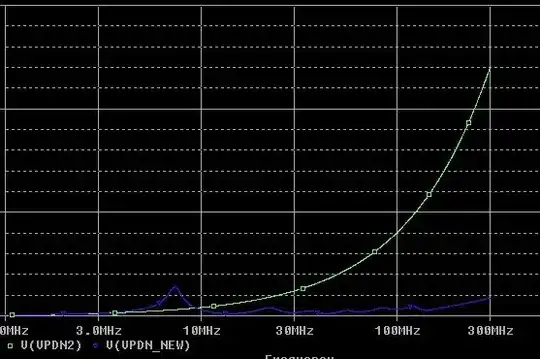
125M-LVDS-wrt-Gnd 125MHz_Circuit

Voltage Spike
  • 75,799
  • 36
  • 80
  • 208
  • 2
    So you see noise but, do you get data corruption? – Andy aka Dec 19 '16 at 13:54
  • What would the scope shot look like if it was taken at a switching frequency of something else than 125MHz? – 12Lappie Dec 19 '16 at 14:37
  • @Andyaka, this LVDS signal is connected to a PLL of Virtex-5 (Xilinx FPGA). PLL keeps on losing lock. – Sachin Vaish Dec 19 '16 at 15:04
  • 3
    First question, how are you grounding those scope probes, two inches of wire and a crocodile clip by any chance? There is something common mode going on and poor scope probe technique seems most likely. I am also not seeing decoupling caps near that osc and buffer... – Dan Mills Dec 19 '16 at 18:56
  • You need to lose your assumptions about the cause of the problem, and include enough information before anyone can answer your question I see the buffer inputs, but relative to what ground? I understand the lower waveform is switcher noise, but two points are you measuring? What is that voltage appearing across? Also, you need to attach the buffer output. And your LVDS signal looks undistorted to me. You have some common mode ground bounce, It's a differential signal, distortion occurs with respect to the opposing polarity line, not ground. – metacollin Feb 20 '17 at 12:54
  • "This is a multi-layer board with adequate layer/return path on board." If this were true, your ground wouldn't be bouncing almost 400mV peak to peak. Though, this shouldn't exceed the common mode range for the buffer... I honestly suspect this isn't an issue with the signal at all, and the PLL is losing lock because of poor decoupling and grounding. In other words, the switching noise is directly causing the problem by screwing with the PLL. I think the LVDS signal is fine - and I think you'll see the buffer output will reflect this. – metacollin Feb 20 '17 at 12:59
  • 1
    +5 for @DanMills if I could. Scope probe pickup or poor power suppy bypassing seem the most likely causes of your (maybe) problem. – The Photon Apr 08 '17 at 15:50

1 Answers1

1

Scale indicates 20ns/div (1div=1cm?) and baud signal looks like 5 symbols or 2.5 square cycles in 20ns or 125MHz (clock? data? )

Spurious resonance is 4 cycles in 20ns thus 200 MHz into 50 Ohms with a Q of ~4 to 5 thus 50 Ohms/4 = Xl=Xc(f) = 15 @200MHz thus 100pF coax capacitance and 15nH

Thus you can now calculate more accurately

Most likely probe ground leads picking up common mode current surge in low ESR cap currents from ground wire.

Use SMA connectors or <<5mm probe pin & gnd and GOOD coax rated for 1GHz.

my quick calculations were from in my head not using calc...

Root cause may be measurement error masking true data errors from crosstalk in PCB tracks and poor balanced impedance from poor differential controlled impedance tracks, connector , cable etc.

Get better measurements first.

Tony Stewart EE75
  • 1
  • 3
  • 54
  • 182