The company I am working for is developing a patient-connected device intended to deliver Functional Electrical Stimulation to a connected user. We are currently struggling to pass the radiated emissions standard.
We have located the source of our problem to our isolated DC/DC power supply by shutting off the isolated power
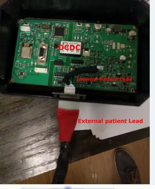
Enclosure
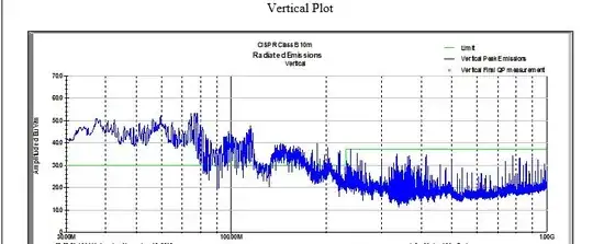
DCDC enabled
DCDC disabled
We also notice that when we disconnect the external patient leads, our radiated emissions are reduced significantly. The signals that we are sending down the cable are biphasic pulses with the following characteristics
- Pulse Width = 500us
- Pulse Amplitude = 150V
- InterPhase Interval = 100us
Frequency = 60hz
 We are in the process of designing a new board with the following features
Get rid of internal patient lead cable in favor of a right angle connector
- Y capacitors across the isolation barrier of the DCDC converter
- Pi filter and Common mode choke on the input of the DCDC converter
- Pi filter at the output of the DCDC converter
- LC filters at the patient connector
However I am still concerned that the external patient cables will radiate excess EMI. Since they are patient cables we are limited on the filtering that we can do and we are not able to shield the cables to the enclosure because it is made of plastic. Does anyone have any suggestions for what we can do to make our device more compliant, specifically as it relates to the patient cables?