1

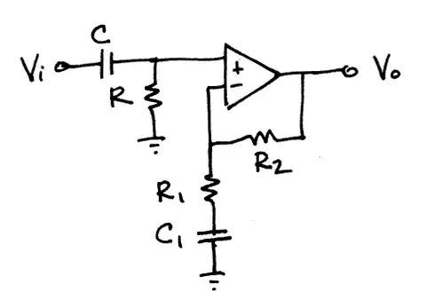
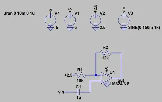
In this non-inverting circuit at page 6 of "A Single-Supply Op-Amp Circuit Collection (SLOA058)":

Schematic 1

I've found out the equation to be (assuming Vcc=+5 V):

$$ Vo=(Vin-2.5)*\frac{R_{1}+R_{2}}{R_{1}}+2.5 $$

Which gives -2.78 V for Vin=0.1V .That cannot be satisfied as this is a single supply operation.

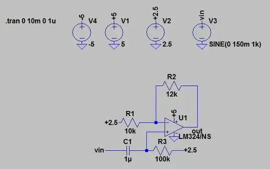
I've verified my equation with this spice simulation with various Vin voltages. It also clips if I give SINE(0 500m 1k) as Vin :

Schematic 2

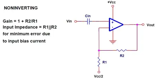
Edit: There is a typo in the above schematic. R2 should go to Vcc/2 instead of GND.

What am I doing wrong? I think there should be a Vcc/2 bias at \$V^{+}\$. But can TI be wrong?

Also when adding a low output impedance Vcc/2 source directly at \$V^{+}\$, it doesn't give the desired effect. You have to put a little big series resistor (100K) after Vcc/2 source. Why is that?

Edit: This is because of the series resistances of the voltage sources, both Vcc/2 and Vin. The series resistances form a voltage divider in-between and preventing you to create a bias; in fact, it will create a bias and almost remove Vin. Still cannot figure out the above question, though.

Edit:

OK, I didn't want to make this a long question. However, there are misunderstandings which are normal because I was in a rush when I asked this question so I was not clear enough.

I am using a model of LM324 instead of an ideal OP-AMP.

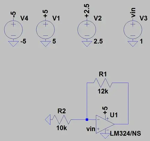
Here is the circuit I think it should be:

First circuit

Graph of first circuit

Here is the circuit in TI paper:

Second circuit

Graph of second circuit

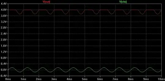
Clearly, there is a bias error.

abdullah kahraman
  • 5,930
  • 7
  • 59
  • 104
  • Out of curiosity, why are you using a dc supply for you Vin? The purpose of the series Cap in the TI figure is to filter out DC range noise on the Op Amp, thus making your SPICE simulation essentially worthless for what you're trying to prove/disprove. – Jeff Langemeier Feb 21 '12 at 16:58
  • Note that R1 and R2 are swapped from the datasheet schematic and your simulation. – tyblu Feb 21 '12 at 17:00
  • I believe he is providing AC content, @JeffLangemeier: "It also clips if I give `SINE(0 500m 1k)` as Vin". – tyblu Feb 21 '12 at 17:02
  • For the simulation to match the app note circuit, 1. Vin should be AC coupled. 2. R2 should connect to Vcc/2, not ground. 3. (Its not 100% clear your doing this) you need to use a full circuit model of the op-amp not an ideal op-amp model. #3 is because you need to have some leakage current through the inputs to set the dc level on the non-inverting input. – The Photon Feb 21 '12 at 17:14
  • 1
    The circuit from the TI app note is wrong and will not work well. There needs to be a DC bias path from the + terminal of the opamp. Otherwise it can float to any DC voltage and the - terminal will be obliged to try to follow it. – markrages Feb 22 '12 at 03:42
  • The circuit was AC coupled when I gave sine input. I am aware that R1 and R2 are swapped. R2 is connected to Vcc/2 as I noted in my edit. I use a full circuit model with input bias currents and etc. Still, the ouput will clip due to wrong DC bias. DC bias should be Vcc/2 not some 3ish volts. – abdullah kahraman Feb 22 '12 at 08:32
  • I think I have found out an answer in [SLOA091](http://www.ti.com/lit/ml/sloa091/sloa091.pdf) page A-9 and A-10. – abdullah kahraman Feb 22 '12 at 09:08
  • Your circuit is incorrect. Your + input has no DC path to a reference ground. So the bias current from that input will charge the capacitor, causing a voltage which will be amplified until the amp is out of range. – Kaz May 18 '12 at 17:08
  • @Kaz which circuit are you referring to? The one after `"Here is the circuit in TI paper:"` ? – abdullah kahraman May 19 '12 at 17:11
  • @abdullahkahraman That comment was about the very first one. – Kaz May 19 '12 at 17:40
  • @Kaz ah, yes, that is the TI's circuit, which I was thinking was wrong, too. – abdullah kahraman May 19 '12 at 18:37

3 Answers3

5

Like markrages says (and like you did in your second schematic) you need to bias the non-inverting input. The document says that

"the input impedance = R1||R2 for minimum error due to input bias current"

That's how it should be, but they don't do it! If you leave it floating it will assume \$GND\$ or \$V_{CC}\$, depending on the opamp's design. The 100k\$\Omega\$ value you use is not the right one, though. For optimal bias this should be equal to 10k\$\Omega\$||12k\$\Omega\$ = 5.6k\$\Omega\$. This will affect the frequency response, since your input is now a high-pass RC filter, with

\$ F_C = \dfrac{1}{2 \cdot \pi \cdot R \cdot C} \$

This will also be the response of your amplifier if you add a capacitor in the feedback path:

enter image description here

\$R\$ goes to \$V_{CC}/2\$ instead of \$GND\$.

From a DC point of view R1 and C1 aren't present, so the output bias will be the same as the input bias (voltage follower). This way of biasing is preferable over connecting R1 to \$V_{CC}/2\$, because you would have to take the voltage divider resistors into account to calculate R1. That's unless you use a "hard" \$V_{CC}/2\$ with a low impedance, like from a voltage regulator.

Same goes for R. If you do want to use a voltage divider you can use resistor values equal to 2 \$\cdot\$ R, then you can eliminate R altogether.

Equations:

\$ F_C = \dfrac{1}{2 \cdot \pi \cdot R1 \cdot C1} = \dfrac{1}{2 \cdot \pi \cdot R \cdot C} \$

stevenvh
  • 145,145
  • 21
  • 455
  • 667
  • 1
    "The claim in the document that the input impedance = R1||R2 is simply false." -- It's badly worded, but I think they're actually trying to say, "you should drive this using a source with output impedance R1||R2 to minimize errors." Which agrees with the rest of your explanation. – The Photon May 18 '12 at 15:24
  • @ThePhoton - Yeah, I guess you're right. The thing is, they're *saying* it, but they don't *do* it. – stevenvh May 18 '12 at 15:28
0

One must use AC analysis to properly examine this circuit. This makes the VCC/2 terminal, the virtual ground, an AC ground terminal. The AC transfer function is thus:

$$ V_{\text{OUT, AC}}=V_{\text{IN, AC}} \left(1+\frac{R_2}{R_1}\right) $$

Total output voltage includes DC offset and is referenced to the system ground, not virtual ground, so it is 2.5VDC higher. With the resistors you specified, it is linear with inputs from about -1.1V to +1.1V.

tyblu
  • 8,167
  • 6
  • 40
  • 70
-2

It's an error in Figure 3, non-inverting circuit. The (+) input must be biased to Vcc/2 through a suitable resistor.

R1 may be attached to Vcc/2 as shown, or AC coupled to ground.

  • 3
    It may *not* be AC coupled to ground! It's that lack of bias the Vcc/2 must solve. BTW, OP *knows* what's the error in figure 3. Read the question, including the last edit. – stevenvh May 18 '12 at 15:19
  • @stevenvh, Wow, at my first answer, I got -7 just because telling the OP to use his mouth when soldering :) So, well, Ted Sims, don't be frustrated :) – abdullah kahraman May 18 '12 at 16:52
  • In this kind of circuit, your Vcc/2 has to be well bypassed, so if R1 goes to Vcc/2, it is thereby going to AC ground also. If it *only* goes to AC ground, then the DC path from output to input via R2 ensures DC stability (unity gain). But this is different from going to Vcc/2, where you have a specific DC gain from R1 and R2. – Kaz May 18 '12 at 17:19
  • @stevenvh Re: *it [R1] may not be AC coupled to ground*. But in your own answer, you have a diagram where R1 is coupled to AC ground. – Kaz May 18 '12 at 17:22
  • @Kaz - The discussion was about the bias of the non-inverting input. I thought he meant that. If the non-inverting input is properly biased, the output can set the inverting input to the same level if there's a resistive feedback path, regardless of other connections. – stevenvh May 19 '12 at 04:00
  • @abdullah - -7 is nothing. AFAIK the current record is -15, for [this answer](http://electronics.stackexchange.com/a/30578/2064). Same user had also posted another answer which was at -7, but that's been deleted. – stevenvh May 19 '12 at 06:08
  • @stevenvh wow, what does that guy is trying to do? I've been following him and he always seems like getting -1s :) – abdullah kahraman May 19 '12 at 07:15