31

I am planning to use the IRFR5305PBF Power MOSFET (http://www.irf.com/product-info/datasheets/data/irfr5305pbf.pdf) to switch on a load. I have determined that I need an external heatsink with Rthsa < 29 C/W.

How would I go about determining the area of copper on the PCB required to provide a thermal resistance of < 29 C/W?

I have tried searching on Google and the IEEE database, but the articles do not clearly show me how to calculate this.

edit: I am using a 4 layer PCB with 1 oz copper on the top and bottom, and 0.5oz copper for the inner layers.

dla59
  • 347
  • 1
  • 3
  • 12
  • Perhaps you are looking at this the wrong way? Why not use a P-channel device with a lower on-resistance, such as this device: http://www.fairchildsemi.com/pf/FQ/FQPF47P06.html. Or even better, use an N-channel device (if you are using it as a load switch, use a charge pump driver to turn the gate on.) – Thomas O Feb 18 '12 at 11:15

4 Answers4

16

Unfortunately there's no simple answer to your question. There's too many variables in the problem for anyone to have measured or characterized every possible configuration: thickness of the FR4, number of copper plane layers, number of vias between the plane layers, the amount of air flow over the board and the inlet air temperature, the thermal contribution of other nearby parts, etc., etc.

There are standard test methods, but these are hardly relevant to any real situation, mainly because they use just bare FR4 with no copper layers as the heat spreading element. Various vendors have also published values for certain configurations. The datasheet you linked, for example, refers to IRF's AN-994, where they give thermal resistance values for various packages offered by that company. But note that their standard test condition uses 2 oz. copper on the outer layers.

Linear technology is another company that publishes informative thermal results. If you can find one of their parts in the same package as your FET, and check the datasheet, they'll likely give a table of thermal resistance for various sized heat spreaders on the top and bottom layers.

For example, for their DDPAK package, which is not quite the same as the DPAK of your IRF part, they give:

Linear DDPAK thermal values

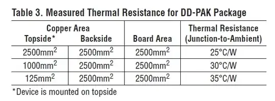
(From the LT1965 datasheet, see there for more detail on the test conditions)

At least you can see that getting to less than 29 C/W is somewhat challenging. The only test conditions in the Linear results that achieved that required 4 square inches of copper on both the top and bottom layers.

But again, you can only count on these figures as guidelines, because factors like airflow will strongly influence the actual results in your application.

The Photon
  • 126,425
  • 3
  • 159
  • 304
8

Suggest you look at SMT heat sinks (e.g. this one for DPAK devices from Aavid) as they will meet your specs (with adequate airflow / convection, of course).

As for PCB copper area alone, you can check appnotes like this one from Fairchild, but I suspect from skimming it that the required area is fairly large (>1 square inch) which is probably not a good guarantee of heat sinking.

Jason S
  • 13,950
  • 3
  • 41
  • 68
2

Here is an interesting article that suggests using 4 layers and vias under the device: AN10874 - LFPAK MOSFET thermal design guide - Application note

Ricardo
  • 6,134
  • 19
  • 52
  • 85
David Drysdale
  • 355
  • 1
  • 15
2

Robert Kollman provides a couple of pages to this subject in Constructing Your Power Supply- Layout Considerations in section V - Thermal Considerations.

I never did this by myself, but I remembered this paper. He provides some examples, so I guess you could probably transfer this to your case.

PetPaulsen
  • 2,335
  • 4
  • 22
  • 34