I once came across Atmel App Note AN2508 - AVR182: Zero Cross Detector (not TI, I know - still interesting) that condones such a construction... For zero-cross sensing on mains!
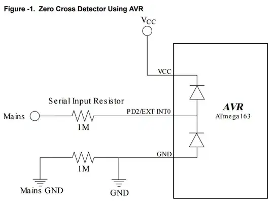
To protect the device from voltages above VCC and below GND, the AVR
has internal clamping diodes on the I/O pins (see Figure -1). The
diodes are connected from the pins to VCC and GND and keep all input
signals within the AVR’s operating voltage (see the figure below). Any
voltage higher than VCC + 0.5V will be forced down to VCC + 0.5V (0.5V
is the voltage drop over the diode) and any voltage below GND -
0.5V will be forced up to GND - 0.5V.
...
The series input resistor is a 1MΩ resistor. It is not recommended
that the clamping diodes are conducting more than maximum 1mA, and 1MΩ
will then allow a maximum voltage of approximately 1,000V.
So, apparently Atmel thinks it's okay to use the clamping diodes on their MCUs in this way, up to 1mA. (Although you can argue about the authority of App Notes)
Personally, I'm still not entirely sure what to think of it. On the one hand, if Atmel specifies it's ok to source/sink up to 1mA through the clamping diodes, then I see no problem if you steer well clear of that current (and 30µA would certainly qualify for that). Also, if used this way, you don't actually exceed the voltage specs; the diodes clamp it down, after all.
On the other, is it ok to use the clamping diodes like this? I never found anything about clamping diode current in the datasheets, so the only source for this is an App Note.
So you could try and find documentation from TI specifying the maximum current through the clamping diodes. Maybe they also have information in their datasheets or App Notes allowing or disallowing these usages.
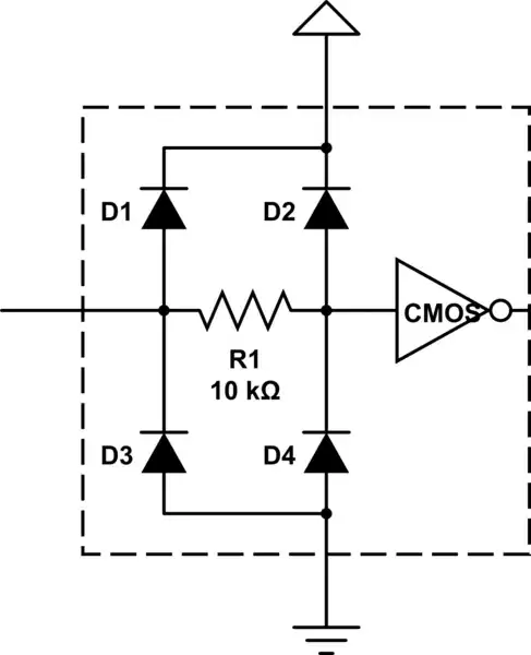
But if you want to be safe, you're better off adding your own clamping diodes, preferably low-Vf ones, i.e. Schottkys. Or use a simple voltage divider. That way you won't have to worry if you're violating the specs or not.
Update, January 2023
When I came across the app note in this answer, I was actually making a hobby project where I ended up using this construct for mains zero-cross sensing. (For some more details, including a schematic, see this question; it's R8/R9).
The circuit connects 230VAC through 2MΩ directly to PB3 on an ATTiny85, putting about 58µA RMS / 163µA peak through the ESD diodes. I'm still not entirely sure how to feel about the whole thing; my motivation for using it was that the project was in part an exercise in minimalism; seeing how far I could reduce the circuit and still have it work well.
Whatever the feelings, over six years of extensive use later, the MCU is still working fine.
Make of that what you will ¯\_(ツ)_/¯