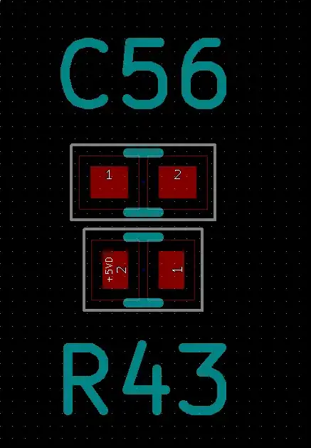
KiCad's default library footprint for C_0402 is longer than R_0402. Why?

Asked
Active
Viewed 3,268 times
9
pericynthion
- 6,164
- 20
- 34
-
402 is 2:1 aspect ratio... your bottom one is not, top is correct – Tony Stewart EE75 Oct 12 '16 at 15:36
-
I think I'll go with the answer below - both are correct, unless you have references to quote... – Sean Houlihane Oct 12 '16 at 15:38
-
don't assume Rpad is correct considering body aspect ratio is wrong – Tony Stewart EE75 Oct 12 '16 at 15:54
-
Btw. Quadratic vs. non quadratic pads is sometimes a good heuristic in figuring out knocked off components in repair jobs – PlasmaHH Oct 12 '16 at 19:01
1 Answers
18
IPC-7351 specifies wider land patterns for chip capacitors than chip resistors, because capacitors are usually taller, so the solder fillet "wants" to extend further laterally. Using the slimmer resistor footprint with a capacitor can lead to reduced assembly yield due to tombstoning.
pericynthion
- 6,164
- 20
- 34
-
1check heights ... it is essential that the solder fillet be limited to 2/3rds of the overall height of the MLC termination, extended pad size allows for this target not to be exceeded ref IPC-SM-782A “Surface Mount Design and Land Pattern Standard”. – Tony Stewart EE75 Oct 12 '16 at 15:39
-
Consider also that the larger footprint allows more solder paste to be applied since solder paste stencils usually use the footprint gerber. In order to save space you might actually reduce the capacitor footprint but modify the stencil with a thicker stencil in capacitor areas to deposit an adequate amount of paste. – Adam Davis Oct 12 '16 at 18:14
-
IPC pads are not intended to be optimal, just the starting point to tune to manufacturers preferred standards for high yields based on chips, orientation , wave vs reflow, Don't blindly use 402 pads without knowing consequences. – Tony Stewart EE75 Oct 13 '16 at 03:21