11

Currently, I have a problem about the Buck-Boost converter. The schematic of my Buck-Boost converter can be seen as below:

The schematic of my Buck-Boost converter

I used the Hall Effect transducers, LV25-P and LA25-NP, to measure the input voltage and input current for the Buck-Boost. Then, the signal are measured by the transducers and sent to the signal condition circuit (right of this figure). For the signal condition circuit, I used LM358 to make the voltage followers. Finally, the signal are sent to ADCs.

The IGBT that I used is IRG4PH50U. The driver is TLP250. The power supplier for TLP250 is +15V, and its ground refers as "Middle". The switch frequency is 20KHz.

I used the PV emulator, Chroma ATE-62050H-600S, as the input source for the Buck-Boost. The output is connceted with a electronic resistance at 20 Omh. I maintained the duty cycle of the IGBT at 49%. The results are shown as below:

where the channel 1 refers the singal at the port "LA", which is in the front of the signal condition circuit. channel 2 refers to the singal at the port "1", which is at the end of the signal condition circuit with a LC lowpass filter. Channel 3 is the input current I measure by the current oscilloscope probe.

The results are not very good. I really want to remove these spikes. Recently, I read some documents about ground bounce, such as What is causing large oscillations in my DC/DC boost converter? Is this ground bounce or some other effect? I assmued that it is caused by ground bounce. However, I do not how to solve it.

Any help would be very appreciated.


Hello, @BruceAbbott. Yes, I have 3 grounds.

One ground is related to transducers and LM358, and I marked it as "triangle". The second ground is related to the driver, TLP250, I marked as "D_GND". The third one is the ground for Buck-Boost, I marked as "GND". I used 0 Omh resistants to connect them together, as you can see in the right part of the figure. When I measured the signals in channel 1 and channel 2, the ground that I connected is P6.

As the request for @PlasmaHH, I added the prototype and the PCB layout.

Prototype PCB Layout


Recently, I tried the solution from @PlasmaHH, and the results are shown as below:

enter image description here

The channel 3 is is the input current I measure by the current oscilloscope probe. The channel 1 and the channel 2 refers the same port, port"1". However, the channel 1 used the ground antenna, while the channel 2 did not. We can see that some ripples are reduced, but not all of them.

I also tried my Boost circuit, which is my previous work. The results are shown as below:

enter image description here

where the channel 1 used the ground antenna, while the channel 2 did not. From this figure, we can see that all of the ripples are reduced.

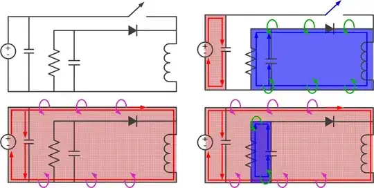
From the discussion above, I think @PlasmaHH is right, but not the whole. @carloc and @rioraxe provided some solutions, and I think they may wokr. I read the airticle by Jeff Barrow, http://www.analog.com/library/analogdialogue/archives/41-06/ground_bounce.html. I think the ground bounce is the culprit. I did some anaylsis for my Buck-Boost, as shown below:

enter image description here

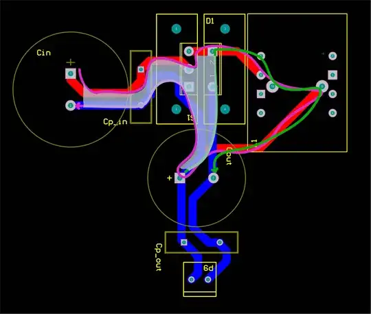
These figures give the two different current loops when the switch is on or off. From this figure, it can be seen the changes of the current loop areas. I proposed a solution to design the PCB layout, as shown below:

enter image description here

The reason I want to used this layout is that I found the current direction for the two current loops are same. Therefore, I only need to think how to redcue the pink area and the green area.

enter image description here

Here is my PCB layout, which is not finished yet. I just want to know whether it works.

enter image description here

The pink lines refer to the current loop when the switch is on, and the green lines refer to the switch is off. The white area is the changes of the current loops.

So, everyone, do you think is OK?

———————————————————————————————————————————— Hello, I made some new changes. Firstly, I reduce the size of the capcitor, because I found I do not really need that big one. Then, I reduce the trace between the inductor GND and Cout. Is this effective to reduce the stray inductances"?

enter image description here


Hi, I just updated my PCB layout. Could you help me to check it?

enter image description here


I made some changes:

  1. Made the IGBT and the diode in one heatsink to reduse the loop area.
  2. Made some components on the bottom side, but I really dont know if it is OK.
  3. Connect the grounds together, as the white circles I marked in the figure.

enter image description here

I donot know how to measure the ESR for caps. But I checked some ducuments about it. It says:

"The input cap is 100V 470uF. Its ESR is 0.06 Ohm. The output cap is 250V 47uF. It ESR is 0.6 Ohm."


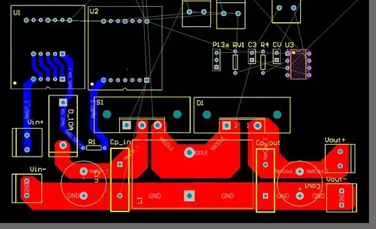
Recently, I made the new PCB board, as shonw below:

enter image description here enter image description here

The result is fine as shown below:

enter image description here

The spike for the input current is smaller. However, I am not sure whether I can make a further improvement.

By the way, I also tested the output current and voltage, as shown below:

enter image description here

Why the waveform output is so weird? How to improve this? Please help me to see it.
Lecio
  • 151
  • 1
  • 7
  • You appear to have 3 separate grounds. How are they connected together physically? Which point was the scope connected to? Show your layout. – Bruce Abbott Sep 13 '16 at 11:30
  • Also show how you connected the probes (i.e.if you used the ground antenna or a proper low inductance connection) – PlasmaHH Sep 13 '16 at 11:32
  • Hello, @BruceAbbott. Yes, I have 3 grounds. One ground is related to transducers and LM358, and I marked it as "triangle". The second ground is related to the driver, TLP250, I marked as "D_GND". The third one is the ground for Buck-Boost, I marked as "GND". I used 0 Omh resistants to connect them together, as you can see in the right part of the figure. When I measured the signals in channel 1 and channel 2, the ground that I connected is P6. I am so sorry that I cannot update the PCB layout because I am new register. So I cannot update more figures in my question. – Lecio Sep 14 '16 at 02:40
  • Hello, @PlasmaHH. I used the common oscilloprobe. I am not sure about "ground antenna" or "proper low inductance connection". I can only describe my ground probe: it is a short wire with a alligator clip. – Lecio Sep 14 '16 at 02:51
  • 1
    @Lecio: yep, that wire is quite a little antenna. Use the low inductance ground spring attachment for your probe and Google about gnd inductance and probes – PlasmaHH Sep 14 '16 at 06:36
  • 2
    Also pcb layout do not help. The two loops depicted here [link](https://dl.dropboxusercontent.com/u/25163354/Cattura.JPG) carry high, fast switching current. They introduce quite some stray inductance which is then prone to oscillate with stray caps. But, even worst, they will induce noise just anywhere in nearby circuits. Those connection should be only made with heavy copper areas, always trying to have go and return paths each on top of the other on two layers. – carloc Sep 14 '16 at 12:00
  • 1
    [1] With switching circuits, bigger is not necessarily better because of higher capacitance and parasitic elements. Try using MOSFET and output diode of more appropriate voltage rating (i.e. not 1200V). [2] electrolytic caps have high ESR, try adding some ceramic caps of a few uF range in parallel with Cout and Cin. [3] Try patching in a thick wire from Cout+ pin directly to inductor pin, that reduces the switching current loop areas. – rioraxe Sep 15 '16 at 04:59
  • Your PCB will "not" work. You much keep all stray inductances to a minimum. Given enough voltage margin an no regard for EMI, it may transfer power from the input to the output just fine but it's down to what you define as "work". – winny Sep 20 '16 at 10:42
  • Hello, @winny, is "stray inductances" same as "parasitic inductance"? – Lecio Sep 21 '16 at 03:30
  • @Lecio In this case yes. – winny Sep 21 '16 at 06:38
  • Still lacking ground plane. But better due to shorter distances. Also, what's the ESR of the capacitors you are using? – winny Sep 22 '16 at 05:34
  • Hi, @winny. What is the "ground plane"? Do you mean "copper plane"? By the way, I donot know the ESR of my capacitors. – Lecio Sep 22 '16 at 05:42
  • Low stray inductance in the PCB and low ESR in your capacitors are vital for any switch mode design. Please see http://www.analog.com/library/analogDialogue/archives/43-09/EDch%2012%20pc%20issues.pdf, http://electronics.stackexchange.com/questions/216116/how-do-i-design-correctly-ground-plane-separation-for-texas-instruments-tps63060 and http://www.ti.com/lit/an/szza009/szza009.pdf. Check the datasheet for your capacitors. Simulate your circuit with paracitics before producing the PCB. Unless you need energy hold-up, you are probably better off with plastic than electolytic caps. – winny Sep 22 '16 at 06:43
  • Hi,@winny, I just updated my PCB layout. Could you help me to check it? – Lecio Sep 28 '16 at 11:50
  • @Lecio Getting better and better. The assumption that the area which the circulating current circomference is equal to your stray inductance isn't really true but a good starting point. Could you have your GND path as the entire bottom of the board? What's the ESR of the input and output caps? Are the electrolytics contributing at all? Can you mount the MOSFET and diode on the same heatsink and much closer to each other? Perhaps even a double-sided heatsink with one on each side if that helps to reduce the length. – winny Sep 28 '16 at 11:58
  • Hi, @winny, I made the new one. Please help me see it~ – Lecio Oct 01 '16 at 12:44
  • Again, better, but I would still like to see a ground plane on the bottom side instead of a separate ground track on the top side. The overall distance from plastic input cap-IGBT-inductor-diode-output plastic cap is short, which is very good. How much current do you plan to run? How much inductance do you have? Let's say 10 A output current and 0.6 ohm, that's 6 V voltage ripple right of the bat. Again, you will most likley be better of with a large plastic cap and no electrolytic on both input and output side. Put in all values, including ESR in a simulator and you will see. – winny Oct 01 '16 at 19:00
  • Hi,@winny, (1) my system runs about 1A to 3.5A current. (2) inductance is 1mH. (3) I have two caps for input and output respectively. I have one electrolytic cap (100V 470uF) and ceramic cap (1000V, 0.1uF), because the parallelled ceramic cap can reduce the ESR. I have three questions now: (1). What do you mean about the "a ground plane on the bottom side instead of a separate ground track on the top side." I donot really understand. (2). The plastic cap is the fime cap? (3). Do I need to use the plastic cap to replace my electrolytic cap? – Lecio Oct 02 '16 at 08:23

2 Answers2

1

First of all, you should be sure that you measure correctly. Your probe has ground antenna effect, you can read the "Measuring Output Ripple and Switching Transients in Switching Regulators" application note, for more detail.

Second, ultra fast diodes trr<=30ns will help your spike problem. To find low ESR capacitors, also you can select high ripple current / high temperature capacitors; for example 105°C capacitors can help your problem. Your PCB also looks like it has parasitic capacitance problem. You can fill with Gnd plane bottom of switch, it reduces parasitic capacitance.

SamGibson
  • 17,231
  • 5
  • 37
  • 58
mr. derecik
  • 71
  • 1
  • 2
0

Your Spikes appear to be starting at IGBT turn on .In your set up the inductor current is quite high at turn on .Most convertors are set up this way so it would be blasphemous of me to say that this is wrong .This continious mode setup needs a fast diode as m derecik said .Also you must slow down the gate turn on of the IGBT by any means .The commonly seen gate resistor is easy to understand and try . Bypass the experimental gate resistor with a fast small diode so IGBT turn off is not slowed.This will burn up some more power but at your chosen 20KHz it should be workable .The gate resistor does depend on your PCB layout .The better your board is the less gate resistance needed to bring spikes to an acceptable level .You could start with a 47 ohm resistor with a BAV21 diode in parallel .If you experiment you will get better waveforms and its always preferable to reduce the spikes by not making them in the first place .Filtering can be difficult because LC components are less ideal at the typical spike oscillation frequencies .You should include some peak current limiting in your design to protect the IGBT better .What I have done commercially to stop turn on spikes is to use a switching regime that basicly turns on the device when the current in the diode is zero and the voltage across the switch is low or zero or slightly negative .

Autistic
  • 14,235
  • 2
  • 27
  • 65